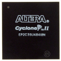
EP2C35U484I8N Altera, EP2C35U484I8N Datasheet - Page 54

EP2C35U484I8N
Manufacturer Part Number
EP2C35U484I8N
Description
IC CYCLONE II FPGA 33K 484-UBGA
Manufacturer
Altera
Series
Cyclone® IIr
Datasheet
1.EP2C5T144C8N.pdf
(168 pages)
Specifications of EP2C35U484I8N
Number Of Logic Elements/cells
33216
Number Of Labs/clbs
2076
Total Ram Bits
483840
Number Of I /o
322
Voltage - Supply
1.15 V ~ 1.25 V
Mounting Type
Surface Mount
Operating Temperature
-40°C ~ 100°C
Package / Case
484-UBGA
For Use With
P0301 - DE2 CALL FOR ACADEMIC PRICING544-1733 - PCI KIT W/CYCLONE II EP2C35N
Lead Free Status / RoHS Status
Lead free / RoHS Compliant
Number Of Gates
-
Other names
544-2115
Available stocks
Company
Part Number
Manufacturer
Quantity
Price
- Current page: 54 of 168
- Download datasheet (3Mb)
I/O Structure & Features
Figure 2–24. Control Signal Selection per IOE
2–42
Cyclone II Device Handbook, Volume 1
Dedicated I/O
Clock [5..0]
Local
Interconnect
Local
Interconnect
Local
Interconnect
Local
Interconnect
Local
Interconnect
Local
Interconnect
io_coe
io_csclr
io_caclr
io_cce_out
io_cce_in
io_cclk
In normal bidirectional operation, you can use the input register for input
data requiring fast setup times. The input register can have its own clock
input and clock enable separate from the OE and output registers. You can
use the output register for data requiring fast clock-to-output
performance. The OE register is available for fast clock-to-output enable
timing. The OE and output register share the same clock source and the
same clock enable source from the local interconnect in the associated
LAB, dedicated I/O clocks, or the column and row interconnects. All
registers share sclr and aclr, but each register can individually disable
sclr and aclr.
configuration.
clk_in
Figure 2–25
clk_out
shows the IOE in bidirectional
ce_in
ce_out
aclr/preset
Altera Corporation
sclr/preset
February 2007
oe
Related parts for EP2C35U484I8N
Image
Part Number
Description
Manufacturer
Datasheet
Request
R

Part Number:
Description:
CYCLONE II STARTER KIT EP2C20N
Manufacturer:
Altera
Datasheet:

Part Number:
Description:
CPLD, EP610 Family, ECMOS Process, 300 Gates, 16 Macro Cells, 16 Reg., 16 User I/Os, 5V Supply, 35 Speed Grade, 24DIP
Manufacturer:
Altera Corporation
Datasheet:

Part Number:
Description:
CPLD, EP610 Family, ECMOS Process, 300 Gates, 16 Macro Cells, 16 Reg., 16 User I/Os, 5V Supply, 15 Speed Grade, 24DIP
Manufacturer:
Altera Corporation
Datasheet:

Part Number:
Description:
Manufacturer:
Altera Corporation
Datasheet:

Part Number:
Description:
CPLD, EP610 Family, ECMOS Process, 300 Gates, 16 Macro Cells, 16 Reg., 16 User I/Os, 5V Supply, 30 Speed Grade, 24DIP
Manufacturer:
Altera Corporation
Datasheet:

Part Number:
Description:
High-performance, low-power erasable programmable logic devices with 8 macrocells, 10ns
Manufacturer:
Altera Corporation
Datasheet:

Part Number:
Description:
High-performance, low-power erasable programmable logic devices with 8 macrocells, 7ns
Manufacturer:
Altera Corporation
Datasheet:

Part Number:
Description:
Classic EPLD
Manufacturer:
Altera Corporation
Datasheet:

Part Number:
Description:
High-performance, low-power erasable programmable logic devices with 8 macrocells, 10ns
Manufacturer:
Altera Corporation
Datasheet:

Part Number:
Description:
Manufacturer:
Altera Corporation
Datasheet:

Part Number:
Description:
Manufacturer:
Altera Corporation
Datasheet:

Part Number:
Description:
Manufacturer:
Altera Corporation
Datasheet:

Part Number:
Description:
CPLD, EP610 Family, ECMOS Process, 300 Gates, 16 Macro Cells, 16 Reg., 16 User I/Os, 5V Supply, 25 Speed Grade, 24DIP
Manufacturer:
Altera Corporation
Datasheet:


