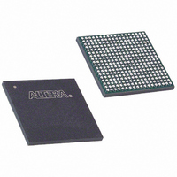
EP1C20F324I7 Altera, EP1C20F324I7 Datasheet - Page 69

EP1C20F324I7
Manufacturer Part Number
EP1C20F324I7
Description
IC CYCLONE FPGA 20K LE 324-FBGA
Manufacturer
Altera
Series
Cyclone®r
Datasheet
1.EP1C3T144C8.pdf
(106 pages)
Specifications of EP1C20F324I7
Number Of Logic Elements/cells
20060
Number Of Labs/clbs
2006
Total Ram Bits
294912
Number Of I /o
233
Voltage - Supply
1.425 V ~ 1.575 V
Mounting Type
Surface Mount
Operating Temperature
-40°C ~ 100°C
Package / Case
324-FBGA
Family Name
Cyclone®
Number Of Logic Blocks/elements
20060
# I/os (max)
233
Frequency (max)
320.1MHz
Process Technology
0.13um (CMOS)
Operating Supply Voltage (typ)
1.5V
Logic Cells
20060
Ram Bits
294912
Operating Supply Voltage (min)
1.425V
Operating Supply Voltage (max)
1.575V
Operating Temp Range
-40C to 100C
Operating Temperature Classification
Industrial
Mounting
Surface Mount
Pin Count
324
Package Type
FBGA
Lead Free Status / RoHS Status
Contains lead / RoHS non-compliant
Number Of Gates
-
Lead Free Status / Rohs Status
Not Compliant
Other names
544-1041
Available stocks
Company
Part Number
Manufacturer
Quantity
Price
Part Number:
EP1C20F324I7
Manufacturer:
ALTERA/阿尔特拉
Quantity:
20 000
Company:
Part Number:
EP1C20F324I7N
Manufacturer:
ALTERA/31
Quantity:
318
Referenced
Documents
Document
Revision History
Altera Corporation
May 2008
May 2008
v1.4
January 2007
v1.3
August 2005
V1.2
February 2005
V1.1
May 2003 v1.0
Table 3–6. Document Revision History
Document
Date and
Version
Added document to Cyclone Device Handbook.
Minor textual and style changes. Added
Documents”
●
●
Minor updates.
Updated JTAG chain limits. Added information concerning test
vectors.
Added document revision history.
Updated handpara note below
Multiple Cyclone devices can be configured in any of the three
configuration schemes by connecting the configuration enable (nCE) and
configuration enable output (nCEO) pins on each device.
This chapter references the following document:
■
■
Table 3–6
Active serial
Passive serial (PS)
JTAG
section.
Table 3–5. Data Sources for Configuration
Configuration Scheme
AN 39: IEEE Std. 1149.1 (JTAG) Boundary-Scan Testing in Altera Devices
Jam Programming & Test Language Specification
shows the revision history for this chapter.
Changes Made
Table
“Referenced
3–4.
Low-cost serial configuration device
Enhanced or EPC2 configuration device,
MasterBlaster or ByteBlasterMV download cable,
or serial data source
MasterBlaster or ByteBlasterMV download cable
or a microprocessor with a Jam or JBC file
Data Source
Referenced Documents
Summary of Changes
—
—
—
—
—
Preliminary
3–7


