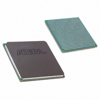
EP2S60F672C4N Altera, EP2S60F672C4N Datasheet - Page 110

EP2S60F672C4N
Manufacturer Part Number
EP2S60F672C4N
Description
IC STRATIX II FPGA 60K 672-FBGA
Manufacturer
Altera
Series
Stratix® IIr
Datasheet
1.EP2S15F484I4N.pdf
(238 pages)
Specifications of EP2S60F672C4N
Number Of Logic Elements/cells
60440
Number Of Labs/clbs
3022
Total Ram Bits
2544192
Number Of I /o
492
Voltage - Supply
1.15 V ~ 1.25 V
Mounting Type
Surface Mount
Operating Temperature
0°C ~ 85°C
Package / Case
672-FBGA
Family Name
Stratix II
Number Of Logic Blocks/elements
60440
# I/os (max)
492
Frequency (max)
711.24MHz
Process Technology
90nm (CMOS)
Operating Supply Voltage (typ)
1.2V
Logic Cells
60440
Ram Bits
2544192
Operating Supply Voltage (min)
1.15V
Operating Supply Voltage (max)
1.25V
Operating Temp Range
0C to 85C
Operating Temperature Classification
Commercial
Mounting
Surface Mount
Pin Count
672
Package Type
FC-FBGA
For Use With
544-1700 - DSP KIT W/STRATIX II EP2S60N544-1697 - NIOS II KIT W/STRATIX II EP2S60N
Lead Free Status / RoHS Status
Lead free / RoHS Compliant
Number Of Gates
-
Lead Free Status / Rohs Status
Compliant
Other names
544-1913
EP2S60F672C4N
EP2S60F672C4N
Available stocks
Company
Part Number
Manufacturer
Quantity
Price
Company:
Part Number:
EP2S60F672C4N
Manufacturer:
ALTERA
Quantity:
3 000
- Current page: 110 of 238
- Download datasheet (3Mb)
High-Speed Differential I/O with DPA Support
Figure 2–60. Fast PLL & Channel Layout in the EP2S15 & EP2S30 Devices
Note to
(1)
2–102
Stratix II Device Handbook, Volume 1
4
See
2
2
Figure
Table 2–21
4
4
2–60:
PLL 1
PLL 2
Fast
Fast
LVDS
LVDS
Clock
Clock
for the number of channels each device supports.
For high-speed source synchronous interfaces such as POS-PHY 4,
Parallel RapidIO, and HyperTransport, the source synchronous clock rate
is not a byte- or SERDES-rate multiple of the data rate. Byte alignment is
necessary for these protocols since the source synchronous clock does not
provide a byte or word boundary since the clock is one half the data rate,
not one eighth. The Stratix II device’s high-speed differential I/O
circuitry provides dedicated data realignment circuitry for user-
controlled byte boundary shifting. This simplifies designs while saving
ALM resources. You can use an ALM-based state machine to signal the
shift of receiver byte boundaries until a specified pattern is detected to
indicate byte alignment.
Fast PLL & Channel Layout
The receiver and transmitter channels are interleaved such that each I/O
bank on the left and right side of the device has one receiver channel and
one transmitter channel per LAB row.
channel layout in the EP2S15 and EP2S30 devices.
fast PLL and channel layout in the EP2S60 to EP2S180 devices.
Clock
Clock
DPA
DPA
Quadrant
Quadrant
Quadrant
Quadrant
Figure 2–60
Clock
Clock
DPA
DPA
Note (1)
shows the fast PLL and
Figure 2–61
LVDS
LVDS
Clock
Clock
Altera Corporation
PLL 4
PLL 3
Fast
Fast
4
4
shows the
May 2007
2
2
4
Related parts for EP2S60F672C4N
Image
Part Number
Description
Manufacturer
Datasheet
Request
R

Part Number:
Description:
CYCLONE II STARTER KIT EP2C20N
Manufacturer:
Altera
Datasheet:

Part Number:
Description:
CPLD, EP610 Family, ECMOS Process, 300 Gates, 16 Macro Cells, 16 Reg., 16 User I/Os, 5V Supply, 35 Speed Grade, 24DIP
Manufacturer:
Altera Corporation
Datasheet:

Part Number:
Description:
CPLD, EP610 Family, ECMOS Process, 300 Gates, 16 Macro Cells, 16 Reg., 16 User I/Os, 5V Supply, 15 Speed Grade, 24DIP
Manufacturer:
Altera Corporation
Datasheet:

Part Number:
Description:
Manufacturer:
Altera Corporation
Datasheet:

Part Number:
Description:
CPLD, EP610 Family, ECMOS Process, 300 Gates, 16 Macro Cells, 16 Reg., 16 User I/Os, 5V Supply, 30 Speed Grade, 24DIP
Manufacturer:
Altera Corporation
Datasheet:

Part Number:
Description:
High-performance, low-power erasable programmable logic devices with 8 macrocells, 10ns
Manufacturer:
Altera Corporation
Datasheet:

Part Number:
Description:
High-performance, low-power erasable programmable logic devices with 8 macrocells, 7ns
Manufacturer:
Altera Corporation
Datasheet:

Part Number:
Description:
Classic EPLD
Manufacturer:
Altera Corporation
Datasheet:

Part Number:
Description:
High-performance, low-power erasable programmable logic devices with 8 macrocells, 10ns
Manufacturer:
Altera Corporation
Datasheet:

Part Number:
Description:
Manufacturer:
Altera Corporation
Datasheet:

Part Number:
Description:
Manufacturer:
Altera Corporation
Datasheet:

Part Number:
Description:
Manufacturer:
Altera Corporation
Datasheet:

Part Number:
Description:
CPLD, EP610 Family, ECMOS Process, 300 Gates, 16 Macro Cells, 16 Reg., 16 User I/Os, 5V Supply, 25 Speed Grade, 24DIP
Manufacturer:
Altera Corporation
Datasheet:


