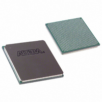
EP1S25F780C5 Altera, EP1S25F780C5 Datasheet - Page 195

EP1S25F780C5
Manufacturer Part Number
EP1S25F780C5
Description
IC STRATIX FPGA 25K LE 780-FBGA
Manufacturer
Altera
Series
Stratix®r
Datasheet
1.EP1S10F780C7.pdf
(276 pages)
Specifications of EP1S25F780C5
Number Of Logic Elements/cells
25660
Number Of Labs/clbs
2566
Total Ram Bits
1944576
Number Of I /o
597
Voltage - Supply
1.425 V ~ 1.575 V
Mounting Type
Surface Mount
Operating Temperature
0°C ~ 85°C
Package / Case
780-FBGA
Family Name
Stratix
Number Of Logic Blocks/elements
25660
# I/os (max)
597
Frequency (max)
500MHz
Process Technology
0.13um (CMOS)
Operating Supply Voltage (typ)
1.5V
Logic Cells
25660
Ram Bits
1944576
Operating Supply Voltage (min)
1.425V
Operating Supply Voltage (max)
1.575V
Operating Temp Range
0C to 85C
Operating Temperature Classification
Commercial
Mounting
Surface Mount
Pin Count
780
Package Type
FC-FBGA
Lead Free Status / RoHS Status
Contains lead / RoHS non-compliant
Number Of Gates
-
Lead Free Status / Rohs Status
Not Compliant
Other names
544-1120
Available stocks
Company
Part Number
Manufacturer
Quantity
Price
Company:
Part Number:
EP1S25F780C5
Manufacturer:
AT
Quantity:
186
Company:
Part Number:
EP1S25F780C5
Manufacturer:
ALTERA
Quantity:
315
Company:
Part Number:
EP1S25F780C5
Manufacturer:
ALTERA
Quantity:
3 000
Company:
Part Number:
EP1S25F780C5AA
Manufacturer:
ALTERA
Quantity:
269
Company:
Part Number:
EP1S25F780C5N
Manufacturer:
ALTERA
Quantity:
3 000
Altera Corporation
January 2006
t
t
t
t
t
t
t
t
t
t
t
t
t
t
t
t
t
t
t
t
t
t
t
t
M4KDATAAH
M4KADDRASU
M4KADDRAH
M4KDATABSU
M4KDATABH
M4KADDRBSU
M4KADDRBH
M4KDATACO1
M4KDATACO2
M4KCLKHL
M4KCLR
MRAMRC
MRAMWC
MRAMWERESU
MRAMWEREH
MRAMCLKENSU
MRAMCLKENH
MRAMBESU
MRAMBEH
MRAMDATAASU
MRAMDATAAH
MRAMADDRASU
MRAMADDRAH
MRAMDATABSU
Table 4–41. M4K Block Internal Timing Microparameter Descriptions (Part
2 of 2)
Table 4–42. M-RAM Block Internal Timing Microparameter
Descriptions (Part 1 of 2)
Symbol
Symbol
A port data hold time after clock
A port address setup time before clock
A port address hold time after clock
B port data setup time before clock
B port data hold time after clock
B port address setup time before clock
B port address hold time after clock
Clock-to-output delay when using output registers
Clock-to-output delay without output registers
Register minimum clock high or low time. This is a limit on
the min time for the clock on the registers in these blocks.
The actual performance is dependent upon the internal
point-to-point delays in the blocks and may give slower
performance as shown
reported by the timing analyzer in the Quartus II software.
Minimum clear pulse width
Synchronous read cycle time
Synchronous write cycle time
Write or read enable setup time before clock
Write or read enable hold time after clock
Clock enable setup time before clock
Clock enable hold time after clock
Byte enable setup time before clock
Byte enable hold time after clock
A port data setup time before clock
A port data hold time after clock
A port address setup time before clock
A port address hold time after clock
B port setup time before clock
Stratix Device Handbook, Volume 1
inTable 4–36 on page 4–20
Parameter
Parameter
DC & Switching Characteristics
and as
4–25


