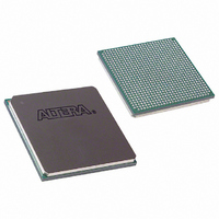
EP1S25F780C5 Altera, EP1S25F780C5 Datasheet - Page 265

EP1S25F780C5
Manufacturer Part Number
EP1S25F780C5
Description
IC STRATIX FPGA 25K LE 780-FBGA
Manufacturer
Altera
Series
Stratix®r
Datasheet
1.EP1S10F780C7.pdf
(276 pages)
Specifications of EP1S25F780C5
Number Of Logic Elements/cells
25660
Number Of Labs/clbs
2566
Total Ram Bits
1944576
Number Of I /o
597
Voltage - Supply
1.425 V ~ 1.575 V
Mounting Type
Surface Mount
Operating Temperature
0°C ~ 85°C
Package / Case
780-FBGA
Family Name
Stratix
Number Of Logic Blocks/elements
25660
# I/os (max)
597
Frequency (max)
500MHz
Process Technology
0.13um (CMOS)
Operating Supply Voltage (typ)
1.5V
Logic Cells
25660
Ram Bits
1944576
Operating Supply Voltage (min)
1.425V
Operating Supply Voltage (max)
1.575V
Operating Temp Range
0C to 85C
Operating Temperature Classification
Commercial
Mounting
Surface Mount
Pin Count
780
Package Type
FC-FBGA
Lead Free Status / RoHS Status
Contains lead / RoHS non-compliant
Number Of Gates
-
Lead Free Status / Rohs Status
Not Compliant
Other names
544-1120
Available stocks
Company
Part Number
Manufacturer
Quantity
Price
Company:
Part Number:
EP1S25F780C5
Manufacturer:
AT
Quantity:
186
Company:
Part Number:
EP1S25F780C5
Manufacturer:
ALTERA
Quantity:
315
Company:
Part Number:
EP1S25F780C5
Manufacturer:
ALTERA
Quantity:
3 000
Company:
Part Number:
EP1S25F780C5AA
Manufacturer:
ALTERA
Quantity:
269
Company:
Part Number:
EP1S25F780C5N
Manufacturer:
ALTERA
Quantity:
3 000
Altera Corporation
January 2006
t
f
% spread
t
t
F I G
f
f
f
f
t
t
t
f
f
t
t
t
t
SKEW
SS
ARESET
A R E S E T _ R E C O N
IN
INPFD
INDUTY
EINDUTY
INJITTER
EINJITTER
FCOMP
OUT
OUT_EXT
OUTDUTY
JITTER
CONFIG5,6
CONFIG11,12
Table 4–127. Enhanced PLL Specifications for -5 Speed Grades (Part 2 of 2)
Table 4–128. Enhanced PLL Specifications for -6 Speed Grades
Symbol
Symbol
Input clock frequency
Input frequency to PFD
Input clock duty cycle
External feedback clock input duty
cycle
Input clock period jitter
External feedback clock period jitter
External feedback clock compensation
time
Output frequency for internal global or
regional clock
Output frequency for external clock
Duty cycle for external clock output
(when set to 50%)
Period jitter for external clock output
(6)
Time required to reconfigure the scan
chains for PLLs 5 and 6
Time required to reconfigure the scan
chains for PLLs 11 and 12
(4)
Clock skew between two external
clock outputs driven by the different
counters with the same settings
Spread spectrum modulation
frequency
Percentage spread for spread
spectrum frequency
Minimum pulse width on
signal
Minimum pulse width on the
areset
reconfiguration. Reset the PLL after
scandataout
Parameter
signal when using PLL
Parameter
goes high.
(10)
areset
(3)
(1),
Min
0.3
0.3
40
40
45
3
3
(2)
Min
500
0.4
30
10
Typ
±75
Typ
0.5
±20 mUI for <200-MHz outclk
±100 ps for >200-MHz outclk
(Part 1 of 2)
Stratix Device Handbook, Volume 1
DC & Switching Characteristics
289/f
193/f
±200
±200
Max
650
420
450
500
60
60
55
SCANCLK
SCANCLK
6
Max
150
0.6
(3)
(3)
ps or
MHz
MHz
MHz
MHz
Unit
mUI
Unit
kHz
ps
ps
ns
%
%
%
ps
ns
ns
4–95
%


