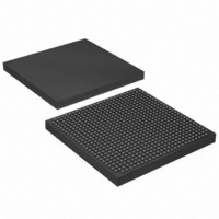
EP1S20F672I7 Altera, EP1S20F672I7 Datasheet - Page 42

EP1S20F672I7
Manufacturer Part Number
EP1S20F672I7
Description
IC STRATIX FPGA 20K LE 672-FBGA
Manufacturer
Altera
Series
Stratix®r
Datasheet
1.EP1S10F780C7.pdf
(276 pages)
Specifications of EP1S20F672I7
Number Of Logic Elements/cells
18460
Number Of Labs/clbs
1846
Total Ram Bits
1669248
Number Of I /o
426
Voltage - Supply
1.425 V ~ 1.575 V
Mounting Type
Surface Mount
Operating Temperature
-40°C ~ 100°C
Package / Case
672-FBGA
Family Name
Stratix
Number Of Logic Blocks/elements
18460
# I/os (max)
426
Frequency (max)
420.17MHz
Process Technology
0.13um (CMOS)
Operating Supply Voltage (typ)
1.5V
Logic Cells
18460
Ram Bits
1669248
Operating Supply Voltage (min)
1.425V
Operating Supply Voltage (max)
1.575V
Operating Temp Range
-40C to 100C
Operating Temperature Classification
Industrial
Mounting
Surface Mount
Pin Count
672
Package Type
FBGA
Lead Free Status / RoHS Status
Contains lead / RoHS non-compliant
Number Of Gates
-
Lead Free Status / Rohs Status
Not Compliant
Available stocks
Company
Part Number
Manufacturer
Quantity
Price
Part Number:
EP1S20F672I7
Manufacturer:
ALTERA/阿尔特拉
Quantity:
20 000
Company:
Part Number:
EP1S20F672I7N
Manufacturer:
ALTERA20
Quantity:
212
- Current page: 42 of 276
- Download datasheet (4Mb)
TriMatrix Memory
2–28
Stratix Device Handbook, Volume 1
M512 RAM blocks can have different clocks on its inputs and outputs.
The wren, datain, and write address registers are all clocked together
from one of the two clocks feeding the block. The read address, rden, and
output registers can be clocked by either of the two clocks driving the
block. This allows the RAM block to operate in read/write or
input/output clock modes. Only the output register can be bypassed. The
eight labclk signals or local interconnect can drive the inclock,
outclock, wren, rden, inclr, and outclr signals. Because of the
advanced interconnect between the LAB and M512 RAM blocks, LEs can
also control the wren and rden signals and the RAM clock, clock enable,
and asynchronous clear signals.
control signal generation logic.
The RAM blocks within Stratix devices have local interconnects to allow
LEs and interconnects to drive into RAM blocks. The M512 RAM block
local interconnect is driven by the R4, R8, C4, C8, and direct link
interconnects from adjacent LABs. The M512 RAM blocks can
communicate with LABs on either the left or right side through these row
interconnects or with LAB columns on the left or right side with the
column interconnects. Up to 10 direct link input connections to the M512
RAM block are possible from the left adjacent LABs and another
10 possible from the right adjacent LAB. M512 RAM outputs can also
connect to left and right LABs through 10 direct link interconnects. The
M512 RAM block has equal opportunity for access and performance to
and from LABs on either its left or right side.
RAM block to logic array interface.
Figure 2–15
shows the M512 RAM block
Figure 2–16
Altera Corporation
shows the M512
July 2005
Related parts for EP1S20F672I7
Image
Part Number
Description
Manufacturer
Datasheet
Request
R

Part Number:
Description:
CYCLONE II STARTER KIT EP2C20N
Manufacturer:
Altera
Datasheet:

Part Number:
Description:
CPLD, EP610 Family, ECMOS Process, 300 Gates, 16 Macro Cells, 16 Reg., 16 User I/Os, 5V Supply, 35 Speed Grade, 24DIP
Manufacturer:
Altera Corporation
Datasheet:

Part Number:
Description:
CPLD, EP610 Family, ECMOS Process, 300 Gates, 16 Macro Cells, 16 Reg., 16 User I/Os, 5V Supply, 15 Speed Grade, 24DIP
Manufacturer:
Altera Corporation
Datasheet:

Part Number:
Description:
Manufacturer:
Altera Corporation
Datasheet:

Part Number:
Description:
CPLD, EP610 Family, ECMOS Process, 300 Gates, 16 Macro Cells, 16 Reg., 16 User I/Os, 5V Supply, 30 Speed Grade, 24DIP
Manufacturer:
Altera Corporation
Datasheet:

Part Number:
Description:
High-performance, low-power erasable programmable logic devices with 8 macrocells, 10ns
Manufacturer:
Altera Corporation
Datasheet:

Part Number:
Description:
High-performance, low-power erasable programmable logic devices with 8 macrocells, 7ns
Manufacturer:
Altera Corporation
Datasheet:

Part Number:
Description:
Classic EPLD
Manufacturer:
Altera Corporation
Datasheet:

Part Number:
Description:
High-performance, low-power erasable programmable logic devices with 8 macrocells, 10ns
Manufacturer:
Altera Corporation
Datasheet:

Part Number:
Description:
Manufacturer:
Altera Corporation
Datasheet:

Part Number:
Description:
Manufacturer:
Altera Corporation
Datasheet:

Part Number:
Description:
Manufacturer:
Altera Corporation
Datasheet:

Part Number:
Description:
CPLD, EP610 Family, ECMOS Process, 300 Gates, 16 Macro Cells, 16 Reg., 16 User I/Os, 5V Supply, 25 Speed Grade, 24DIP
Manufacturer:
Altera Corporation
Datasheet:


