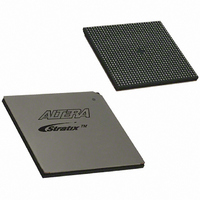
EP1S30B956C5 Altera, EP1S30B956C5 Datasheet - Page 112

EP1S30B956C5
Manufacturer Part Number
EP1S30B956C5
Description
IC STRATIX FPGA 30K LE 956-BGA
Manufacturer
Altera
Series
Stratix®r
Datasheet
1.EP1S10F780C7.pdf
(276 pages)
Specifications of EP1S30B956C5
Number Of Logic Elements/cells
32470
Number Of Labs/clbs
3247
Total Ram Bits
3317184
Number Of I /o
683
Voltage - Supply
1.425 V ~ 1.575 V
Mounting Type
Surface Mount
Operating Temperature
0°C ~ 85°C
Package / Case
956-BGA
Lead Free Status / RoHS Status
Contains lead / RoHS non-compliant
Number Of Gates
-
Available stocks
Company
Part Number
Manufacturer
Quantity
Price
Company:
Part Number:
EP1S30B956C5N
Manufacturer:
ALTERA
Quantity:
280
- Current page: 112 of 276
- Download datasheet (4Mb)
PLLs & Clock Networks
2–98
Stratix Device Handbook, Volume 1
f
The variation due to process, voltage, and temperature is about ±15% on
the delay settings. PLL reconfiguration can control the clock delay shift
elements, but not the VCO phase shift multiplexers, during system
operation.
Spread-Spectrum Clocking
Stratix device enhanced PLLs use spread-spectrum technology to reduce
electromagnetic interference generation from a system by distributing the
energy over a broader frequency range. The enhanced PLL typically
provides 0.5% down spread modulation using a triangular profile. The
modulation frequency is programmable. Enabling spread-spectrum for a
PLL affects all of its outputs.
Lock Detect
The lock output indicates that there is a stable clock output signal in
phase with the reference clock. Without any additional circuitry, the lock
signal may toggle as the PLL begins tracking the reference clock. You may
need to gate the lock signal for use as a system control. The lock signal
from the locked port can drive the logic array or an output pin.
Whenever the PLL loses lock (for example, inclk jitter, clock switchover,
PLL reconfiguration, power supply noise, and so on), the PLL must be
reset with the areset signal to guarantee correct phase relationship
between the PLL output clocks. If the phase relationship between the
input clock versus output clock, and between different output clocks
from the PLL is not important in the design, then the PLL need not be
reset.
See the Stratix FPGA Errata Sheet for more information on implementing
the gated lock signal in a design.
Programmable Duty Cycle
The programmable duty cycle allows enhanced PLLs to generate clock
outputs with a variable duty cycle. This feature is supported on each
enhanced PLL post-scale counter (g0..g3, l0..l3, e0..e3). The duty cycle
setting is achieved by a low and high time count setting for the post-scale
dividers. The Quartus II software uses the frequency input and the
required multiply or divide rate to determine the duty cycle choices.
Advanced Clear & Enable Control
There are several control signals for clearing and enabling PLLs and their
outputs. You can use these signals to control PLL resynchronization and
gate PLL output clocks for low-power applications.
Altera Corporation
July 2005
Related parts for EP1S30B956C5
Image
Part Number
Description
Manufacturer
Datasheet
Request
R

Part Number:
Description:
CYCLONE II STARTER KIT EP2C20N
Manufacturer:
Altera
Datasheet:

Part Number:
Description:
CPLD, EP610 Family, ECMOS Process, 300 Gates, 16 Macro Cells, 16 Reg., 16 User I/Os, 5V Supply, 35 Speed Grade, 24DIP
Manufacturer:
Altera Corporation
Datasheet:

Part Number:
Description:
CPLD, EP610 Family, ECMOS Process, 300 Gates, 16 Macro Cells, 16 Reg., 16 User I/Os, 5V Supply, 15 Speed Grade, 24DIP
Manufacturer:
Altera Corporation
Datasheet:

Part Number:
Description:
Manufacturer:
Altera Corporation
Datasheet:

Part Number:
Description:
CPLD, EP610 Family, ECMOS Process, 300 Gates, 16 Macro Cells, 16 Reg., 16 User I/Os, 5V Supply, 30 Speed Grade, 24DIP
Manufacturer:
Altera Corporation
Datasheet:

Part Number:
Description:
High-performance, low-power erasable programmable logic devices with 8 macrocells, 10ns
Manufacturer:
Altera Corporation
Datasheet:

Part Number:
Description:
High-performance, low-power erasable programmable logic devices with 8 macrocells, 7ns
Manufacturer:
Altera Corporation
Datasheet:

Part Number:
Description:
Classic EPLD
Manufacturer:
Altera Corporation
Datasheet:

Part Number:
Description:
High-performance, low-power erasable programmable logic devices with 8 macrocells, 10ns
Manufacturer:
Altera Corporation
Datasheet:

Part Number:
Description:
Manufacturer:
Altera Corporation
Datasheet:

Part Number:
Description:
Manufacturer:
Altera Corporation
Datasheet:

Part Number:
Description:
Manufacturer:
Altera Corporation
Datasheet:

Part Number:
Description:
CPLD, EP610 Family, ECMOS Process, 300 Gates, 16 Macro Cells, 16 Reg., 16 User I/Os, 5V Supply, 25 Speed Grade, 24DIP
Manufacturer:
Altera Corporation
Datasheet:


