EP1S30B956C5 Altera, EP1S30B956C5 Datasheet - Page 194
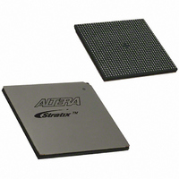
EP1S30B956C5
Manufacturer Part Number
EP1S30B956C5
Description
IC STRATIX FPGA 30K LE 956-BGA
Manufacturer
Altera
Series
Stratix®r
Datasheet
1.EP1S10F780C7.pdf
(276 pages)
Specifications of EP1S30B956C5
Number Of Logic Elements/cells
32470
Number Of Labs/clbs
3247
Total Ram Bits
3317184
Number Of I /o
683
Voltage - Supply
1.425 V ~ 1.575 V
Mounting Type
Surface Mount
Operating Temperature
0°C ~ 85°C
Package / Case
956-BGA
Lead Free Status / RoHS Status
Contains lead / RoHS non-compliant
Number Of Gates
-
Available stocks
Company
Part Number
Manufacturer
Quantity
Price

Company:
Part Number:
EP1S30B956C5N
Manufacturer:
ALTERA
Quantity:
280


Timing Model
4–24
Stratix Device Handbook, Volume 1
t
t
t
t
t
t
t
t
t
t
t
t
t
t
t
t
t
t
t
t
t
t
t
t
t
M512RC
M512WC
M512WERESU
M512WEREH
M512CLKENSU
M512CLKENH
M512DATASU
M512DATAH
M512WADDRSU
M512WADDRH
M512RADDRSU
M512RADDRH
M512DATACO1
M512DATACO2
M512CLKHL
M512CLR
M4KRC
M4KWC
M4KWERESU
M4KWEREH
M4KCLKENSU
M4KCLKENH
M4KBESU
M4KBEH
M4KDATAASU
Table 4–40. M512 Block Internal Timing Microparameter Descriptions
Table 4–41. M4K Block Internal Timing Microparameter Descriptions (Part
1 of 2)
Symbol
Symbol
Synchronous read cycle time
Synchronous write cycle time
Write or read enable setup time before clock
Write or read enable hold time after clock
Clock enable setup time before clock
Clock enable hold time after clock
Data setup time before clock
Data hold time after clock
Write address setup time before clock
Write address hold time after clock
Read address setup time before clock
Read address hold time after clock
Clock-to-output delay when using output registers
Clock-to-output delay without output registers
Register minimum clock high or low time. This is a limit on
the min time for the clock on the registers in these blocks.
The actual performance is dependent upon the internal
point-to-point delays in the blocks and may give slower
performance as shown in
reported by the timing analyzer in the Quartus II software.
Minimum clear pulse width
Synchronous read cycle time
Synchronous write cycle time
Write or read enable setup time before clock
Write or read enable hold time after clock
Clock enable setup time before clock
Clock enable hold time after clock
Byte enable setup time before clock
Byte enable hold time after clock
A port data setup time before clock
Parameter
Parameter
Table 4–36 on page 4–20
Altera Corporation
January 2006
and as
Related parts for EP1S30B956C5
Image
Part Number
Description
Manufacturer
Datasheet
Request
R

Part Number:
Description:
CYCLONE II STARTER KIT EP2C20N
Manufacturer:
Altera
Datasheet:


Part Number:
Description:
CPLD, EP610 Family, ECMOS Process, 300 Gates, 16 Macro Cells, 16 Reg., 16 User I/Os, 5V Supply, 35 Speed Grade, 24DIP
Manufacturer:
Altera Corporation
Datasheet:
Part Number:
Description:
CPLD, EP610 Family, ECMOS Process, 300 Gates, 16 Macro Cells, 16 Reg., 16 User I/Os, 5V Supply, 15 Speed Grade, 24DIP
Manufacturer:
Altera Corporation
Datasheet:
Part Number:
Description:
Manufacturer:
Altera Corporation
Datasheet:
Part Number:
Description:
CPLD, EP610 Family, ECMOS Process, 300 Gates, 16 Macro Cells, 16 Reg., 16 User I/Os, 5V Supply, 30 Speed Grade, 24DIP
Manufacturer:
Altera Corporation
Datasheet:
Part Number:
Description:
High-performance, low-power erasable programmable logic devices with 8 macrocells, 10ns
Manufacturer:
Altera Corporation
Datasheet:
Part Number:
Description:
High-performance, low-power erasable programmable logic devices with 8 macrocells, 7ns
Manufacturer:
Altera Corporation
Datasheet:
Part Number:
Description:
Classic EPLD
Manufacturer:
Altera Corporation
Datasheet:
Part Number:
Description:
High-performance, low-power erasable programmable logic devices with 8 macrocells, 10ns
Manufacturer:
Altera Corporation
Datasheet:
Part Number:
Description:
Manufacturer:
Altera Corporation
Datasheet:
Part Number:
Description:
Manufacturer:
Altera Corporation
Datasheet:
Part Number:
Description:
Manufacturer:
Altera Corporation
Datasheet:
Part Number:
Description:
CPLD, EP610 Family, ECMOS Process, 300 Gates, 16 Macro Cells, 16 Reg., 16 User I/Os, 5V Supply, 25 Speed Grade, 24DIP
Manufacturer:
Altera Corporation
Datasheet: