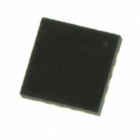
CY8C20246A-24LKXI Cypress Semiconductor Corp, CY8C20246A-24LKXI Datasheet - Page 21

CY8C20246A-24LKXI
Manufacturer Part Number
CY8C20246A-24LKXI
Description
MCU 16K FLASH 2K SRAM 16UQFN
Manufacturer
Cypress Semiconductor Corp
Series
CapSense® Controllersr
Specifications of CY8C20246A-24LKXI
Program Memory Type
FLASH (16 kB)
Package / Case
16-UQFN, 16-µQFN
Applications
Capacitive Sensing
Core Processor
M8C
Controller Series
CY8C20xx6A
Ram Size
2K x 8
Interface
I²C, SPI
Number Of I /o
13
Voltage - Supply
1.71 V ~ 5.5 V
Operating Temperature
-40°C ~ 85°C
Mounting Type
Surface Mount
Processor Series
CY8C20x46A
Core
M8C
Data Bus Width
8 bit
Data Ram Size
2 KB
Interface Type
I2C, SPI
Maximum Clock Frequency
24 MHz
Number Of Programmable I/os
10
Number Of Timers
3
Operating Supply Voltage
1.71 V to 5.5 V
Maximum Operating Temperature
+ 85 C
Mounting Style
SMD/SMT
Development Tools By Supplier
CY3280-20X66
Minimum Operating Temperature
- 40 C
Program Memory Size
16 KB
Operating Temperature (min)
-40C
Operating Temperature (max)
85C
Application
CapSense
Processing Unit
Microprocessor
Operating Supply Voltage (min)
1.71V
Operating Supply Voltage (typ)
1.8/2.5/3.3/5V
Operating Supply Voltage (max)
5.5V
Package Type
QFN
Pin Count
16
Mounting
Surface Mount
Rad Hardened
No
Lead Free Status / RoHS Status
Lead free / RoHS Compliant
For Use With
770-1000 - ISP 4PORT FOR CYPRESS PSOC MCU
Lead Free Status / Rohs Status
Lead free / RoHS Compliant
Table 16. 2.4V to 3.0V DC GPIO Specifications
Table 17. 1.71V to 2.4V DC GPIO Specifications
Document Number: 001-54459 Rev. **
R
V
V
V
V
V
V
V
V
V
V
I
C
R
V
V
V
V
V
V
V
IL
Symbol
Symbol
OH1
OH2
OH3
OH4
OH5A
OH6A
OL
IL
IH
H
OH1
OH2
OH3
OH4
OL
IL
IH
PU
PIN
PU
Pull up Resistor
High Output Voltage
Port 2 or 3 Pins
High Output Voltage
Port 2 or 3 Pins
High Output Voltage
Port 0 or 1 Pins with LDO Regulator
Disabled for Port 1
High Output Voltage
Port 0 or 1 Pins with LDO Regulator
Disabled for Port 1
Low Output Voltage
Input Low Voltage
Input High Voltage
Pull up Resistor
High Output Voltage
Port 2 or 3 Pins
High Output Voltage
Port 2 or 3 Pins
High Output Voltage
Port 0 or 1 Pins with LDO Regulator
Disabled for Port 1
High Output Voltage
Port 0 or 1 Pins with LDO Regulator
Disabled for Port 1
High Output Voltage
Port 1 Pins with LDO Enabled for 1.8V
Out
High Output Voltage
Port 1 Pins with LDO Enabled for 1.8V
Out
Low Output Voltage
Input Low Voltage
Input High Voltage
Input Hysteresis Voltage
Input Leakage (Absolute Value)
Capacitive Load on Pins
Description
Description
IOH = 10 μA, maximum of 10 mA
source current in all I/Os
IOH = 0.5 mA, maximum of 10 mA
source current in all I/Os
IOH = 100 μA, maximum of 10 mA
source current in all I/Os
IOH = 2 mA, maximum of 10 mA source
current in all I/Os
IOL = 5 mA, maximum of 20 mA sink
current on even port pins (for example,
P0[2] and P1[4]) and 30 mA sink
current on odd port pins (for example,
P0[3] and P1[5])
IOH < 10 μA, maximum of 10 mA
source current in all IOs
IOH = 0.2 mA, maximum of 10 mA
source current in all IOs
IOH < 10 μA, maximum of 10 mA
source current in all IOs
IOH = 2 mA, maximum of 10 mA source
current in all IOs
IOH < 10 μA, Vdd > 2.4V, maximum of
20 mA source current in all IOs
IOH = 1 mA, Vdd > 2.4V, maximum of
20 mA source current in all IOs
IOL = 10 mA, maximum of 30 mA sink
current on even port pins (for example,
P0[2] and P1[4]) and 30 mA sink
current on odd port pins (for example,
P0[3] and P1[5])
Package and pin dependent
Temp = 25
o
C
Conditions
Conditions
CY8C20X36A/46A/66A/96A
0.65 x Vdd
Vdd - 0.2
Vdd - 0.5
Vdd - 0.2
Vdd - 0.5
Vdd - 0.2
Vdd - 0.4
Vdd - 0.2
Vdd - 0.5
Min
1.50
1.20
Min
1.4
0.5
4
–
–
–
–
–
–
4
0.001
1.80
Typ
Typ
5.6
5.6
1.7
80
–
–
–
–
–
–
–
–
–
–
–
–
–
–
–
0.3 x Vdd
Max
0.75
0.72
Max
2.1
0.4
8
–
–
–
–
–
–
1
5
8
–
–
–
–
Page 21 of 38
Units
Units
mV
kΩ
kΩ
μA
pF
V
V
V
V
V
V
V
V
V
V
V
V
V
V
V
V
[+] Feedback


