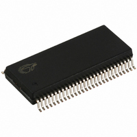
CY7C66113C-PVXC Cypress Semiconductor Corp, CY7C66113C-PVXC Datasheet - Page 12

CY7C66113C-PVXC
Manufacturer Part Number
CY7C66113C-PVXC
Description
IC MCU 8K USB HUB 4 PORT 56TSSOP
Manufacturer
Cypress Semiconductor Corp
Specifications of CY7C66113C-PVXC
Applications
USB Hub/Microcontroller
Core Processor
M8
Program Memory Type
OTP (8 kB)
Controller Series
USB Hub
Ram Size
256 x 8
Interface
I²C, USB, HAPI
Number Of I /o
31
Voltage - Supply
4 V ~ 5.5 V
Operating Temperature
0°C ~ 70°C
Mounting Type
Surface Mount
Package / Case
56-SSOP
No. Of I/o's
31
Eeprom Memory Size
8KB
Ram Memory Size
256Byte
Cpu Speed
48MHz
Digital Ic Case Style
SSOP
Supply
RoHS Compliant
Core Size
8bit
Program Memory Size
8KB
Oscillator Type
External, Internal
Peripherals
DAC
Rohs Compliant
Yes
Controller Family/series
(8051) USB
Embedded Interface Type
HAPI, I2C, USB
Processor Series
CY7C66xx
Core
M8
Data Bus Width
16 bit
Data Ram Size
256 B
Interface Type
HAPI, I2C, USB
Maximum Clock Frequency
12 MHz
Number Of Programmable I/os
39
Number Of Timers
1
Maximum Operating Temperature
+ 70 C
Mounting Style
SMD/SMT
Development Tools By Supplier
CY3654, CY3654-P03
Minimum Operating Temperature
0 C
Lead Free Status / RoHS Status
Lead free / RoHS Compliant
For Use With
CY3649 - PROGRAMMER HI-LO USB M8428-1339 - KIT LOW SPEED PERSONALITY BOARD
Lead Free Status / Rohs Status
Details
Other names
428-1808
Available stocks
Company
Part Number
Manufacturer
Quantity
Price
Company:
Part Number:
CY7C66113C-PVXC
Manufacturer:
HITTITE
Quantity:
101
Part Number:
CY7C66113C-PVXC
Manufacturer:
CIRRUS
Quantity:
20 000
8-Bit Accumulator (A)
The accumulator is the general purpose register for the
microcontroller.
8-Bit Temporary Register (X)
The “X” register is available to the firmware for temporary storage
of intermediate results. The microcontroller performs indexed
operations based on the value in X. Refer to the section,
on page 13 for additional information.
8-Bit Program Stack Pointer (PSP)
During a reset, the Program Stack Pointer (PSP) is set to 0x00
and “grows” upward from this address. The PSP may be set by
firmware, using the MOV PSP,A instruction. The PSP supports
interrupt service under hardware control and CALL, RET, and
RETI instructions under firmware control. The PSP is not
readable by the firmware.
During an interrupt acknowledge, interrupts are disabled and the
14-bit program counter, carry flag, and zero flag are written as
two bytes of data memory. The first byte is stored in the memory
addressed by the PSP, then the PSP is incremented. The second
byte is stored in memory addressed by the PSP, and the PSP is
incremented again. The overall effect is to store the program
Table 5. SRAM Areas
8-Bit Data Stack Pointer (DSP)
The Data Stack Pointer (DSP) supports PUSH and POP
instructions that use the data stack for temporary storage. A
PUSH instruction pre-decrements the DSP, then writes data to
the memory location addressed by the DSP. A POP instruction
reads data from the memory location addressed by the DSP,
then post-increments the DSP.
During a reset, the DSP is reset to 0x00. A PUSH instruction
when DSP equals 0x00 writes data at the top of the data RAM
(address 0xFF). This writes data to the memory area reserved
for USB endpoint FIFOs. Therefore, the DSP should be indexed
at an appropriate memory location that does not compromise the
Document Number: 38-08024 Rev. *D
Notes
8-bit DSP
(Move DSP
8-bit DSP
1. Refer to
2. Endpoint sizes are fixed by the Endpoint Size Bit (I/O register 0x1F, Bit 7), see
After Reset
8-Bit Data Stack Pointer (DSP)
[1]
)
8-bit PSP
for a description of DSP.
0x00
User Selected
0xFF
Address
Indexed
User variables
USB FIFO space for up to two addresses and five endpoints
Table
counter and flags on the program “stack” and increment the PSP
by two.
The Return From Interrupt (RETI) instruction decrements the
PSP, then restores the second byte from memory addressed by
the PSP. The PSP is decremented again and the first byte is
restored from memory addressed by the PSP. After the program
counter and flags are restored from stack, the interrupts are
enabled. The overall effect is to restore the program counter and
flags from the program stack, decrement the PSP by two, and
re-enable interrupts.
The Call Subroutine (CALL) instruction stores the program
counter and flags on the program stack and increments the PSP
by two.
The Return From Subroutine (RET) instruction restores the
program counter but not the flags from the program stack and
decrements the PSP by two.
Data Memory Organization
The CY7C66x13C microcontrollers provide 256 bytes of data
RAM. Normally, the SRAM is partitioned into four areas: program
stack, user variables, data stack, and USB endpoint FIFOs. The
following is one example of where the program stack, data stack,
and user variables areas are located.
Program Stack, user defined memory (variables), or the USB
endpoint FIFOs.
For USB applications, the firmware should set the DSP to an
appropriate location to avoid a memory conflict with RAM
dedicated to USB FIFOs. The memory requirements for the USB
endpoints are described in
Example assembly instructions to do this with two device
addresses (FIFOs begin at 0xD8) are shown:
■
■
14.
MOV A,20h; Move 20 hex into Accumulator (must be D8h or
less)
SWAP A,DSP; swap accumulator value into DSP register.
Program Stack Growth
Data Stack Growth
CY7C66013C, CY7C66113C
USB Device Endpoints
Page 12 of 59
on page 38.
[2]
[+] Feedback


