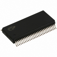
CY7C66113C-PVXC Cypress Semiconductor Corp, CY7C66113C-PVXC Datasheet - Page 27

CY7C66113C-PVXC
Manufacturer Part Number
CY7C66113C-PVXC
Description
IC MCU 8K USB HUB 4 PORT 56TSSOP
Manufacturer
Cypress Semiconductor Corp
Specifications of CY7C66113C-PVXC
Applications
USB Hub/Microcontroller
Core Processor
M8
Program Memory Type
OTP (8 kB)
Controller Series
USB Hub
Ram Size
256 x 8
Interface
I²C, USB, HAPI
Number Of I /o
31
Voltage - Supply
4 V ~ 5.5 V
Operating Temperature
0°C ~ 70°C
Mounting Type
Surface Mount
Package / Case
56-SSOP
No. Of I/o's
31
Eeprom Memory Size
8KB
Ram Memory Size
256Byte
Cpu Speed
48MHz
Digital Ic Case Style
SSOP
Supply
RoHS Compliant
Core Size
8bit
Program Memory Size
8KB
Oscillator Type
External, Internal
Peripherals
DAC
Rohs Compliant
Yes
Controller Family/series
(8051) USB
Embedded Interface Type
HAPI, I2C, USB
Processor Series
CY7C66xx
Core
M8
Data Bus Width
16 bit
Data Ram Size
256 B
Interface Type
HAPI, I2C, USB
Maximum Clock Frequency
12 MHz
Number Of Programmable I/os
39
Number Of Timers
1
Maximum Operating Temperature
+ 70 C
Mounting Style
SMD/SMT
Development Tools By Supplier
CY3654, CY3654-P03
Minimum Operating Temperature
0 C
Lead Free Status / RoHS Status
Lead free / RoHS Compliant
For Use With
CY3649 - PROGRAMMER HI-LO USB M8428-1339 - KIT LOW SPEED PERSONALITY BOARD
Lead Free Status / Rohs Status
Details
Other names
428-1808
Available stocks
Company
Part Number
Manufacturer
Quantity
Price
Company:
Part Number:
CY7C66113C-PVXC
Manufacturer:
HITTITE
Quantity:
101
Part Number:
CY7C66113C-PVXC
Manufacturer:
CIRRUS
Quantity:
20 000
Interrupts
Interrupts are generated by the GPIO and DAC pins, the internal timers, I
on various USB traffic conditions. All interrupts are maskable by the Global Interrupt Enable Register and the USB End Point Interrupt
Enable Register. Writing a ‘1’ to a bit position enables the interrupt associated with that bit position.
Global Interrupt Enable Register
Bit 0: USB Bus RST Interrupt Enable
Bit 1: 128 μs Interrupt Enable
Bit 2: 1.024 ms Interrupt Enable
Bit 3: USB Hub Interrupt Enable
USB Endpoint Interrupt Enable
Bit 0: EPA0 Interrupt Enable
Bit 1: EPA1 Interrupt Enable
Bit 2: EPA2 Interrupt Enable
Bit 3: EPB0 Interrupt Enable
Document Number: 38-08024 Rev. *D
Bit #
Bit Name
Read/Write
Reset
Bit #
Bit Name
Read/Write
Reset
1 = Enable Interrupt on a USB Bus Reset; 0 = Disable
interrupt on a USB Bus Reset (refer to
Interrupt).
1 = Enable Timer interrupt every 128 μs; 0 = Disable Timer
Interrupt for every 128 μs.
1= Enable Timer interrupt every 1.024 ms; 0 = Disable
Timer Interrupt every 1.024 ms.
1 = Enable Interrupt on a Hub status change; 0 = Disable
interrupt due to hub status change. (Refer to
Interrupt.)
1 = Enable Interrupt on data activity through endpoint A0;
0 = Disable Interrupt on data activity through endpoint A0.
1 = Enable Interrupt on data activity through endpoint A1;
0 = Disable Interrupt on data activity through endpoint A1.
1 = Enable Interrupt on data activity through endpoint A2;
0 = Disable Interrupt on data activity through endpoint A2.
1 = Enable Interrupt on data activity through endpoint B0;
0 = Disable Interrupt on data activity through endpoint B0.
7
Reserved
-
-
7
Reserved
-
-
6
I
Enable
R/W
0
6
Reserved
-
-
2
C Interrupt
Figure 30. USB Endpoint Interrupt Enable Register
Figure 29. Global Interrupt Enable Register
5
GPIO
Interrupt
Enable
R/W
0
5
Reserved
-
-
USB Bus Reset
USB Hub
4
DAC
Interrupt
Enable
R/W
0
4
EPB1
Interrupt
Enable
R/W
0
Bit 4: DAC Interrupt Enable
Bit 5: GPIO Interrupt Enable
Bit 6: I
Bit 7: Reserved.
Bit 4: EPB1 Interrupt Enable
Bit [7..5]: Reserved
During a reset, the contents the Global Interrupt Enable Register
and USB End Point Interrupt Enable Register are cleared,
effectively, disabling all interrupts.
The interrupt controller contains a separate flip flop for each
interrupt. See
interrupt controller. When an interrupt is generated, it is first
registered as a pending interrupt. It stays pending until it is
serviced or a reset occurs. A pending interrupt only generates an
interrupt request if it is enabled by the corresponding bit in the
interrupt enable registers. The highest priority interrupt request
2
3
USB Hub
Interrupt
Enable
R/W
0
1 = Enable Interrupt on falling and rising edge on any
GPIO; 0 = Disable Interrupt on falling and rising edge on
any GPIO. (Refer to sections
GPIO Configuration
Ports.)
1 = Enable Interrupt on I2C related activity; 0 = Disable I2C
related activity interrupt. (Refer to
3
Interrupt
Enable
R/W
0
1 = Enable Interrupt on data activity through endpoint B1;
0 = Disable Interrupt on data activity through endpoint B1.
C compatible or HAPI operation, the internal USB hub, or
1 = Enable DAC Interrupt; 0 = Disable DAC interrupt.
EPB0
2
C Interrupt Enable
Figure 31
CY7C66013C, CY7C66113C
2
1.024 ms
Interrupt
Enable
R/W
0
2
EPA2
Interrupt
Enable
R/W
0
for the logic block diagram of the
Port, and
1
128 μs
Interrupt
Enable
R/W
0
1
EPA1
Interrupt
Enable
R/W
0
GPIO and HAPI
GPIO Interrupt Enable
I
2
C
Interrupt.)
ADDRESS 0X20
ADDRESS 0X21
0
USB Bus
RST
Interrupt
Enable
R/W
0
Page 27 of 59
0
EPA0
Interrupt
Enable
R/W
0
Interrupt,
[+] Feedback


