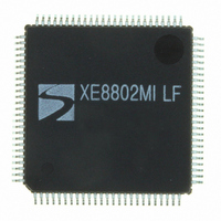
XE8802MI035LF Semtech, XE8802MI035LF Datasheet - Page 159

XE8802MI035LF
Manufacturer Part Number
XE8802MI035LF
Description
IC DAS 16BIT FLASH 8K 100-LQFP
Manufacturer
Semtech
Datasheet
1.XE8802MI035LF.pdf
(193 pages)
Specifications of XE8802MI035LF
Applications
Sensing Machine
Core Processor
RISC
Program Memory Type
FLASH (22 kB)
Controller Series
XE8000
Ram Size
1K x 8
Interface
SPI, UART
Number Of I /o
36
Voltage - Supply
2.4 V ~ 5.5 V
Operating Temperature
-40°C ~ 85°C
Mounting Type
Surface Mount
Package / Case
100-LQFP
For Use With
XE8000MP - PROG BOARD AND PROSTART2 CARD
Lead Free Status / RoHS Status
Lead free / RoHS Compliant
Available stocks
Company
Part Number
Manufacturer
Quantity
Price
Company:
Part Number:
XE8802MI035LF
Manufacturer:
TI
Quantity:
8 700
- Current page: 159 of 193
- Download datasheet (2Mb)
1. To select a frame rate of about 50Hz, set the bits LcdFreq=10 and LcdDivFreq=100 in RegLcdClkFrame. Note
that the precision of the frame frequency depends on the selected clock source (see clock block documentation).
The 120 segments are on or off depending on the bits set in the registers RegLcdDataN. All bits of these registers
are used in 1:4 multiplexing. Figure 19-9 shows the generated waveforms for twelve segments. The segments
connected to pad_lcd_io[0] are all on (LcdData0[3:0]=1111 in RegLcdData0), the segments connected to
pad_lcd_io[1] are all off (LcdData0[7:4]=0000 in RegLcdData0) and the segments connected to pad_lcd_io[2] are
partially on, partially off (LcdData1[2:0]=1101 in RegLcdData1). The figure shows on the left side the waveforms
on the circuit pins, in the middle the segment status and on the right the voltage on some segments (difference
between the pad_lcd_io pin and common signal: pad_lcd_com0, pad_lcd_com1, pad_lcd_io[31] or pad_lcd_io[30]).
19.5 Advanced LCD features
19.5.1
To set the peripheral in LCD mode, all bits in RegLcdSe have to be set to 1.
The status of the segments has to be written to the registers RegLcdDataN (with 0<N<15). Each register drives the
segments connected to the pins pad_lcd_io[2N] (bits 0 to 3) and pad_lcd_io[2N+1] (bits 4 to 7). Depending on the
selected multiplexing (LcdMux in RegLcdOn), not all bits in the data registers RegLcdDataN are used as shown
in Table 19-17. The unused locations will always read back ‘0’. When reading back these registers, it will give the
actual value on the display. When writing to these registers, the modifications will be taken into account only at the
start of a new frame.
Note that in the 1:3 multiplexing, the pad_lcd_io[31] pin is used as the third common signal and the data
LcdData15[7:4] are not used. In the 1:4 multiplexing, the pad_lcd_io[31:30] are used as common signals and the
data LcdData15[7:0] are not used.
In the LCD mode, all pads have LCD driver capabilities. The parallel port configuration registers
(RegPLcdPullupN, RegPLcdDirN and RegPLcdOutN ) are unused. Writing to these registers will have no
influence on the peripheral activity. These registers and RegPLcdInN will read back ‘0’.
19.5.2
When putting the LCD driver in sleep mode (LcdSleep = 1 in RegLcdOn), the peripheral will stop the waveform
generation at the end of a frame. Entering sleep mode does not modify the LCD set-up but during sleep mode, the
user is still allowed to write data into the RegLcdDataN registers. Figure 19-10 shows an example of the sleep
mode synchronisation. The sleep signal can be used to blink the display.
© Semtech 2006
Register usage
Sleep mode or blinking mode
RegLcdDataN[x]
3, 7
2, 6
1, 5
0, 4
XE8802 Sensing Machine Data Acquisition MCU
DD
x
x
x
used
Table 19-17. Useful data.
19-15
1:2
x
x
used
used
with ZoomingADC™ and LCD driver
1:3
x
used
used
used
1:4
used
used
used
used
www.semtech.com
Related parts for XE8802MI035LF
Image
Part Number
Description
Manufacturer
Datasheet
Request
R

Part Number:
Description:
EVALUATION BOARD
Manufacturer:
Semtech
Datasheet:

Part Number:
Description:
EVALUATION BOARD
Manufacturer:
Semtech
Datasheet:

Part Number:
Description:
VOLTAGE SUPPRESSOR, TRANSIENT SEMTECH
Manufacturer:
Semtech
Datasheet:

Part Number:
Description:
HIGH VOLTAGE CAPACITORS MONOLITHIC CERAMIC TYPE
Manufacturer:
Semtech Corporation
Datasheet:

Part Number:
Description:
EZ1084CM5.0 AMP POSITIVE VOLTAGE REGULATOR
Manufacturer:
Semtech Corporation
Datasheet:

Part Number:
Description:
3.0 AMP LOW DROPOUT POSITIVE VOLTAGE REGULATORS
Manufacturer:
Semtech Corporation
Datasheet:

Part Number:
Description:
Manufacturer:
Semtech Corporation
Datasheet:

Part Number:
Description:
RailClamp Low Capacitance TVS Diode Array
Manufacturer:
Semtech Corporation
Datasheet:

Part Number:
Description:
Manufacturer:
Semtech Corporation
Datasheet:

Part Number:
Description:
Manufacturer:
Semtech Corporation
Datasheet:

Part Number:
Description:
Manufacturer:
Semtech Corporation
Datasheet:

Part Number:
Description:
Manufacturer:
Semtech Corporation
Datasheet:


