CY7C63743-SXC Cypress Semiconductor Corp, CY7C63743-SXC Datasheet - Page 16
CY7C63743-SXC
Manufacturer Part Number
CY7C63743-SXC
Description
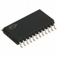
IC MCU 8K USB/PS2 LS 24SOIC
Manufacturer
Cypress Semiconductor Corp
Series
enCoRe™r
Specifications of CY7C63743-SXC
Applications
USB Microcontroller
Core Processor
M8B
Program Memory Type
OTP (8 kB)
Controller Series
CY7C637xx
Ram Size
256 x 8
Interface
PS2, USB
Number Of I /o
16
Voltage - Supply
4 V ~ 5.5 V
Operating Temperature
0°C ~ 70°C
Mounting Type
Surface Mount
Package / Case
24-SOIC (7.5mm Width)
Lead Free Status / RoHS Status
Lead free / RoHS Compliant
Other names
428-1622
Available stocks
Company
Part Number
Manufacturer
Quantity
Price

Part Number:
CY7C63743-SXC
Manufacturer:
CYPRESS/赛普拉斯
Quantity:
20 000


Table 12-1. Ports 0 and 1 Output Control Truth Table
12.1
Port 2 serves as an auxiliary input port as shown in
Figure 12-8. The Port 2 inputs all have TTL input thresholds.
Bit [7:6]: Reserved
Bit [5:4]: D+ (SCLK) and D– (SDATA) States
Bit [3:2]: Reserved
Bit 1: P2.1 (Internal Clock Mode Only)
Bit 0: P2.0/VREG Pin State
Document #: 38-08022 Rev. *B
Name
Read/
Reset
Write
Bit #
Bit
The state of the D+ and D– pins can be read at Port 2 Data
Register. Performing a read from the port pins returns their
logic values.
1 = Port Pin is logic HIGH
0 = Port Pin is logic LOW
In the Internal Clock mode, the XTALIN pin can serve as a
general purpose input, and its state can be read at Port 2,
Bit 1 (P2.1). See Section 9.1 for more details.
1 = Port Pin is logic HIGH
0 = Port Pin is logic LOW
In PS/2 mode, the VREG pin can be used as an input and
its state can be read at port P2.0. Section 15.0 for more
details.
1 = Port Pin is logic HIGH
0 = Port Pin is logic LOW
Register
Figure 12-8. Port 2 Data Register (Address 0x02)
Data
0
1
0
1
0
1
0
1
Reserved
Auxiliary Input Port
7
0
-
6
0
-
Mode1 Mode0 Output Drive
(SCLK)
0
0
1
1
State
D+
R
5
0
(SDATA)
0
1
0
1
State
D–
R
4
0
High (50 mA)
(8 mA) Sink
Low (2 mA)
High Drive
High Drive
Reserved
Strength
Resistive
Medium
3
0
-
Sink
Sink
Hi-Z
Hi-Z
FOR
FOR
2
0
-
(Internal
Clock
Mode
Only)
P2.1
Threshold
R
1
0
CMOS
CMOS
CMOS
CMOS
CMOS
CMOS
CMOS
Input
TTL
VREG
State
P2.0
Pin
R
0
0
13.0
The SIE allows the microcontroller to communicate with the
USB host. The SIE simplifies the interface between the micro-
controller and USB by incorporating hardware that handles the
following USB bus activity independently of the microcon-
troller:
Firmware is required to handle the rest of the USB interface
with the following tasks:
13.1
A typical USB enumeration sequence is shown below. In this
description, ‘Firmware’ refers to embedded firmware in the
CY7C637xx controller.
10.Once the device receives a Set Configuration request, its
11.Firmware should take appropriate action for Endpoint 1
1. The host computer sends a SETUP packet followed by a
2. Firmware decodes the request and retrieves its Device
3. The host computer performs a control read sequence and
4. After receiving the descriptor, the host sends a SETUP
5. Firmware stores the new address in its USB Device
6. The host sends a request for the Device descriptor using
7. Firmware decodes the request and retrieves the Device
8. The host performs a control read sequence and Firmware
9. The host generates control reads from the device to request
• Translate the encoded received data and format the data to
• CRC checking and generation. Flag the microcontroller if
• Address checking. Ignore the transactions not addressed
• Send appropriate ACK/NAK/STALL handshakes.
• Token type identification (SETUP, IN, or OUT). Set the ap-
• Place valid received data in the appropriate endpoint FIFOs.
• Send and update the data toggle bit (Data1/0).
• Bit stuffing/unstuffing.
• Coordinate enumeration by decoding USB device requests.
• Fill and empty the FIFOs.
• Suspend/Resume coordination.
• Verify and select Data toggle values.
be transmitted on the bus.
errors exist during transmission.
to the device.
propriate token bit once a valid token is received.
DATA packet to USB address 0 requesting the Device de-
scriptor.
descriptor from the program memory tables.
Firmware responds by sending the Device descriptor over
the USB bus, via the on-chip FIFO.
packet followed by a DATA packet to address 0 assigning
a new USB address to the device.
Address Register after the no-data control sequence
completes.
the new USB address.
descriptor from program memory tables.
responds by sending its Device descriptor over the USB
bus.
the Configuration and Report descriptors.
functions may now be used.
and/or 2 transactions, which may occur from this point.
USB Enumeration
USB Serial Interface Engine (SIE)
CY7C63722
CY7C63723
CY7C63743
Page 16 of 49
Related parts for CY7C63743-SXC
Image
Part Number
Description
Manufacturer
Datasheet
Request
R

Part Number:
Description:
Manufacturer:
Cypress Semiconductor Corp
Datasheet:
Part Number:
Description:
Manufacturer:
Cypress Semiconductor Corp
Datasheet:
Part Number:
Description:
Manufacturer:
Cypress Semiconductor Corp
Datasheet:
Part Number:
Description:
Manufacturer:
Cypress Semiconductor Corp
Datasheet:
Part Number:
Description:
Manufacturer:
Cypress Semiconductor Corp
Datasheet: