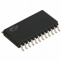
CY7C63743-SXC Cypress Semiconductor Corp, CY7C63743-SXC Datasheet - Page 17

CY7C63743-SXC
Manufacturer Part Number
CY7C63743-SXC
Description
IC MCU 8K USB/PS2 LS 24SOIC
Manufacturer
Cypress Semiconductor Corp
Series
enCoRe™r
Specifications of CY7C63743-SXC
Applications
USB Microcontroller
Core Processor
M8B
Program Memory Type
OTP (8 kB)
Controller Series
CY7C637xx
Ram Size
256 x 8
Interface
PS2, USB
Number Of I /o
16
Voltage - Supply
4 V ~ 5.5 V
Operating Temperature
0°C ~ 70°C
Mounting Type
Surface Mount
Package / Case
24-SOIC (7.5mm Width)
Lead Free Status / RoHS Status
Lead free / RoHS Compliant
Other names
428-1622
Available stocks
Company
Part Number
Manufacturer
Quantity
Price
Part Number:
CY7C63743-SXC
Manufacturer:
CYPRESS/赛普拉斯
Quantity:
20 000
13.2
USB status and control is regulated by the USB Status and
Control Register as shown in Figure 13-1.
Bit 7: PS/2 Pull-up Enable
Bit 6: V
Bit 5: USB-PS/2 Interrupt Select
Note:
Document #: 38-08022 Rev. *B
Name
Read/
Reset
Write
2.
Bit #
Figure 13-1. USB Status and Control Register (Address
Bit
This bit is used to enable the internal PS/2 pull-up resistors
on the SDATA and SCLK pins. Normally the output high
level on these pins is V
clamped to approximately 1 Volt above V
Enable bit is set, or if the Device Address is enabled (bit 7
of the USB Device Address Register, Figure 14-1).
1 = Enable PS/2 Pull-up resistors. The SDATA and SCLK
pins are pulled up internally to V
approximately 5 kΩ (see Section 25.0 for the value of
R
0 = Disable PS/2 Pull-up resistors.
A 3.3V voltage regulator is integrated on chip to provide a
voltage source for a 1.5-kΩ pull-up resistor connected to
the D– pin as required by the USB Specification. Note that
the VREG output has an internal series resistance of ap-
proximately 200Ω, the external pull-up resistor required is
approximately 1.3-kΩ (see Figure 16-1).
1 = Enable the 3.3V output voltage on the VREG pin.
0 = Disable. The VREG pin can be configured as an input.
This bit allows the user to select whether an USB bus reset
interrupt or a PS/2 activity interrupt will be generated when
the interrupt conditions are detected.
For PS/2 operation, the D+/D– Forcing Bit [2:0] = 111b mode must be set initially (one time only) before using the other PS/2 force modes.
PS2
Pull-up
Enable
REG
).
PS/2
R/W
USB Port Status and Control
7
0
Enable
Enable
VREG
R/W
6
0
Interrupt
Activity
Reset-
Mode
PS/2
USB
R/W
5
0
CC
0x1F)
, but note that the output will be
Reserved USB
4
0
-
CC
FOR
FOR
with two resistors of
Activity
R/W
REG
Bus
3
0
if the VREG
0 0 0
Forcing
D+/D–
R/W
2:0
Bit
Bit 4: Reserved. Must be written as a ‘0’.
Bit 3: USB Bus Activity
Bit [2:0]: D+/D– Forcing Bit [2:0]
Table 13-1. Control Modes to Force D+/D– Outputs
D+/D– Forcing
1 = PS/2 interrupt mode. A PS/2 activity interrupt will occur
if the SDATA pin is continuously LOW for 128 to 256 µs.
0 = USB interrupt mode (default state). In this mode, a USB
bus reset interrupt will occur if the single ended zero (SE0,
D– and D+ are LOW) exists for 128 to 256 µs.
See Section 21.3 for more details.
The Bus Activity bit is a “sticky” bit that detects any non-idle
USB event has occurred on the USB bus. Once set to HIGH
by the SIE to indicate the bus activity, this bit retains its
logical HIGH value until firmware clears it. Writing a ‘0’ to
this bit clears it; writing a ‘1’ preserves its value. The user
firmware should check and clear this bit periodically to de-
tect any loss of bus activity. Firmware can clear the Bus
Activity bit, but only the SIE can set it. The 1.024-ms timer
interrupt service routine is normally used to check and clear
the Bus Activity bit.
1 = There has been bus activity since the last time this bit
was cleared. This bit is set by the SIE.
0 = No bus activity since last time this bit was cleared (by
firmware).
Forcing bits allow firmware to directly drive the D+ and D–
pins, as shown in Table 13-1. Outputs are driven with con-
trolled edge rates in these modes for low EMI. For forcing
the D+ and D– pins in USB mode, D+/D– Forcing Bit 2
should be 0. Setting D+/D– Forcing Bit 2 to ‘1’ puts both
pins in an open-drain mode, preferred for applications such
as PS/2 or LED driving.
Bit [2:0]
000
001
010
011
100
101
110
111
Not forcing (SIE controls driver) Any Mode
Force K (D+ HIGH, D– LOW)
Force J (D+ LOW, D– HIGH)
Force SE0 (D– LOW, D+ LOW)
Force D– LOW, D+ LOW
Force D– LOW, D+ HiZ
Force D– HiZ, D+ LOW
Force D– HiZ, D+ HiZ
Control Action
CY7C63722
CY7C63723
CY7C63743
Page 17 of 49
PS/2 Mode
Application
USB Mode
[2]


