MM908E626AVDWB Freescale Semiconductor, MM908E626AVDWB Datasheet - Page 30
MM908E626AVDWB
Manufacturer Part Number
MM908E626AVDWB
Description
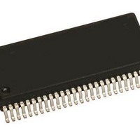
IC STEPPER MOTOR DRIVER 54-SOIC
Manufacturer
Freescale Semiconductor
Type
Stepper Motor Driverr
Datasheet
1.MM908E626AVEK.pdf
(44 pages)
Specifications of MM908E626AVDWB
Applications
Automotive Mirror Control
Core Processor
HC08
Program Memory Type
FLASH (16 kB)
Controller Series
908E
Ram Size
512 x 8
Interface
SCI, SPI
Number Of I /o
13
Voltage - Supply
8 V ~ 18 V
Operating Temperature
-40°C ~ 115°C
Mounting Type
Surface Mount
Package / Case
54-SOIC (7.5mm Width) Exposed Pad, 54-eSOIC, 54-HSOIC
Product
Stepper Motor Controllers / Drivers
Operating Supply Voltage
8 V to 18 V
Supply Current
20 mA
Mounting Style
SMD/SMT
Lead Free Status / Rohs Status
Lead free / RoHS Compliant
Available stocks
Company
Part Number
Manufacturer
Quantity
Price

Part Number:
MM908E626AVDWB
Manufacturer:
FREESCALE
Quantity:
20 000


CSA — H-bridges Current Sense Amplification Select Bit
of the H-bridges. Reset clears the CSA bit.
CLS2 : CLS0 — H-bridge Current Limitation Selection Bits
according to
Switchable VDD Outputs
used for driving external circuitry that requires a V
The output is enabled with bit PSON in the System Control
Register and can be switched on / off with bit HVDDON in the
Power Output Register. Low or high voltage conditions (LVI /
HVDD Over-temperature Protection
temperature reset is enabled.
HVDD Over-current Protection
event the over-current limit is or was reached, the output
automatically switches off and the HVDD over-current flag in
the System Status Register is set.
30
HVI) have no influence on this circuitry.
908E626
FUNCTIONAL DEVICE OPERATION
OPERATIONAL MODES
Table 8. H-bridge Current Limitation Value Selection
CLS2
This read / write bit selects the current sense amplification
• 1 = Current sense amplification set for measuring 0.5 A.
• 0 = Current sense amplification set for measuring 2.5 A.
These read / write bits select the current limitation value
The HVDD pin is a switchable VDD output pin. It can be
Over-temperature protection is enabled if the high
The HVDD output is protected against over-current. In the
0
0
0
0
1
1
1
1
CLS1
Table
0
0
1
1
0
0
1
1
8. Reset clears the CLS2 : CLS0 bits.
CLS0
0
1
0
1
0
1
0
1
Bits
Current Limit
260mA (typ)
370mA (typ)
550mA (typ)
740mA (typ)
55mA (typ)
No Limit
DD
voltage.
System Control Register (SYSCTL)
PSON — Power Stages On Bit
LIN transmitter and HVDD output). Reset clears the PSON
bit.
SRS0 : SRS1 — LIN Slew Rate Selection Bits
appropriate LIN slew rate for different baud rate
configurations as shown in
programming via the LIN and are not intended for use in the
application.
Table 9. LIN Slew Rate Selection Bits
Go to STOP Mode Bit (GS)
and go into STOP mode. Reset or CPU interrupt requests
clear the GS bit.
System Status Register (SYSSTAT)
LINCL — LIN Current Limitation Bit
current limitation region. Due to excessive power dissipation
Reset
Reset
Read
Read
Write
Write
This read / write bit enables the power stages (half-bridges,
• 1 = Power stages enabled.
• 0 = Power stages disabled.
These read / write bits enable the user to select the
The high speed slew rates are used, for example, for
SRS1
This write-only bit instructs the 908E626 to power down
• 1 = Power down and go into STOP mode
• 0 = Not in STOP mode
This read-only bit is set if the LIN transmitter operates in
0
0
1
1
PSON
Bit 7
Bit 7
Register Name and Address: SYSSTAT - $0c
Register Name and Address: SYSCTL - $03
0
0
0
SRS0
LINCL
SRS1
0
1
0
1
6
0
6
0
HVDD
_OCF
SRS0
Analog Integrated Circuit Device Data
5
0
5
0
Table
Initial Slew Rate (20 kBaud)
Slow Slew Rate (10 kBaud)
4
0
0
4
0
0
High Speed II (8 x)
High Speed I (4 x)
9.
LIN Slew Rate
Freescale Semiconductor
LVF
3
0
0
3
0
HVF
2
0
0
2
0
1
0
0
OCF
HB_
1
0
Bit 0
GS
0
0
Bit 0
HTF
0
Related parts for MM908E626AVDWB
Image
Part Number
Description
Manufacturer
Datasheet
Request
R

Part Number:
Description:
Integrated Stepper Motor Driver With Embedded Mcu And Lin Serial Communication
Manufacturer:
Freescale Semiconductor, Inc
Datasheet:
Part Number:
Description:
Manufacturer:
Freescale Semiconductor, Inc
Datasheet:
Part Number:
Description:
Manufacturer:
Freescale Semiconductor, Inc
Datasheet:
Part Number:
Description:
Manufacturer:
Freescale Semiconductor, Inc
Datasheet:
Part Number:
Description:
Manufacturer:
Freescale Semiconductor, Inc
Datasheet:
Part Number:
Description:
Manufacturer:
Freescale Semiconductor, Inc
Datasheet:
Part Number:
Description:
Manufacturer:
Freescale Semiconductor, Inc
Datasheet:
Part Number:
Description:
Manufacturer:
Freescale Semiconductor, Inc
Datasheet:
Part Number:
Description:
Manufacturer:
Freescale Semiconductor, Inc
Datasheet:
Part Number:
Description:
Manufacturer:
Freescale Semiconductor, Inc
Datasheet:
Part Number:
Description:
Manufacturer:
Freescale Semiconductor, Inc
Datasheet:
Part Number:
Description:
Manufacturer:
Freescale Semiconductor, Inc
Datasheet:
Part Number:
Description:
Manufacturer:
Freescale Semiconductor, Inc
Datasheet:
Part Number:
Description:
Manufacturer:
Freescale Semiconductor, Inc
Datasheet:
Part Number:
Description:
Manufacturer:
Freescale Semiconductor, Inc
Datasheet: