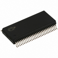
CY7C66113-PVC Cypress Semiconductor Corp, CY7C66113-PVC Datasheet - Page 21

CY7C66113-PVC
Manufacturer Part Number
CY7C66113-PVC
Description
IC MCU 8K USB HUB 4 PORT 56TSSOP
Manufacturer
Cypress Semiconductor Corp
Specifications of CY7C66113-PVC
Applications
USB Hub/Microcontroller
Core Processor
M8
Program Memory Type
OTP (8 kB)
Controller Series
USB Hub
Ram Size
256 x 8
Interface
I²C, USB, HAPI
Number Of I /o
31
Voltage - Supply
4 V ~ 5.5 V
Operating Temperature
0°C ~ 70°C
Mounting Type
Surface Mount
Package / Case
56-SSOP
Operating Temperature (max)
70C
Operating Temperature (min)
0C
Operating Temperature Classification
Commercial
Mounting
Surface Mount
Pin Count
56
Lead Free Status / RoHS Status
Contains lead / RoHS non-compliant
For Use With
CY3649 - PROGRAMMER HI-LO USB M8428-1339 - KIT LOW SPEED PERSONALITY BOARD
Lead Free Status / RoHS Status
Not Compliant, Contains lead / RoHS non-compliant
Other names
428-1330
Available stocks
Company
Part Number
Manufacturer
Quantity
Price
Company:
Part Number:
CY7C66113-PVC
Manufacturer:
CY
Quantity:
10
11.0
HAPI (Hardware Assisted Parallel Interface) provides for a 1, 2, or 3 byte interface to an external device. I
standard interface for Inter-IC Communication. Register 0x09 configures the HAPI and I
HAPI and I
The operation of these interfaces is explained below.
Bits [7,1:0] of the HAPI/I
Latch Empty and Data Ready bits: These bits are an inversion of the respective pins. They exist so that the firmware can
determine what type of operations need to be performed on the HAPI port following an interrupt. Care must be taken to consider
the state of LEMPTY and DRDY polarity signals when reading these bits. For example, following a HAPI interrupt due to an
external device reading data from the HAPI port the DRDY signal will have transitioned from a 1 to a 0. The Data Ready bit will
transition from a 0 to a 1 indicating that the ports need to be reloaded with data for the external device to read.
DRDY and LEMPTY Polarity bits: These bits control the polarity of the output pins. The default polarity is high true. Setting this
bit to a 1 changes the polarity to low true.
Table 11-1. HAPI Port Configuration
I
2
C Position
Port Width Bits[1:0]
R/W
7
HAPI and I
2
C is discussed in Sections 12.0 and 13.0.
11
L3
11
10
01
00
D3
Reserved
10
L2
R/W
6
D2
2
2
C Configuration Register
C Configuration Register control the pin out configuration of the HAPI and I
9
L1
D1
Figure 11-1. HAPI/I
8
L0
24 Bits: P3[7:0], P1[7:0], P0[7:0]
LEMPTY
D0
Polarity
R/W
16 Bits: P1[7:0], P0[7:0]
5
7
PRELIMINARY
No HAPI Interface
HAPI Port Width
D7
8 Bits: P0[7:0]
Figure 10-3. Timer Block Diagram
6
D6
2
C Configuration Register 0x09 (read/write)
Polarity
5
DRDY
R/W
D5
4
4
D4
21
3
Latch Empty
D3
R
3
2
D2
1
D1
Data Ready
8
0
D0
R
2
2
C interfaces. The detailed operation of
1.024-ms Interrupt
128- s Interrupt
1-MHz Clock
To Timer Register
CY7C66011/12/13
CY7C66111/12/13
Width Bit 1
HAPI Port
2
C interfaces.
R/W
1
2
C interface utilizes the
Width Bit 0
HAPI Port
R/W
0


