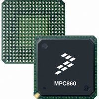
MPC855TCVR50D4 Freescale Semiconductor, MPC855TCVR50D4 Datasheet - Page 11

MPC855TCVR50D4
Manufacturer Part Number
MPC855TCVR50D4
Description
IC MPU POWERQUICC 50MHZ 357PBGA
Manufacturer
Freescale Semiconductor
Datasheets
1.MPC855TVR50D4.pdf
(15 pages)
2.MPC8555ECVTALF.pdf
(88 pages)
3.MPC855TCVR50D4.pdf
(80 pages)
Specifications of MPC855TCVR50D4
Processor Type
MPC8xx PowerQUICC 32-Bit
Speed
50MHz
Voltage
3.3V
Mounting Type
Surface Mount
Package / Case
357-PBGA
Processor Series
MPC8xx
Core
MPC8xx
Data Bus Width
32 bit
Maximum Clock Frequency
50 MHz
Operating Supply Voltage
2.5 V, 3.3 V
Maximum Operating Temperature
+ 95 C
Mounting Style
SMD/SMT
Minimum Operating Temperature
- 40 C
Family Name
MPC8xx
Device Core
PowerQUICC
Device Core Size
32b
Frequency (max)
50MHz
Instruction Set Architecture
RISC
Supply Voltage 1 (typ)
2.5/3.3V
Operating Supply Voltage (max)
3.465/3.6V
Operating Supply Voltage (min)
2/3.135V
Operating Temp Range
-40C to 95C
Operating Temperature Classification
Industrial
Mounting
Surface Mount
Pin Count
357
Package Type
BGA
Lead Free Status / RoHS Status
Lead free / RoHS Compliant
Features
-
Lead Free Status / Rohs Status
Lead free / RoHS Compliant
Available stocks
Company
Part Number
Manufacturer
Quantity
Price
Company:
Part Number:
MPC855TCVR50D4
Manufacturer:
FREESCAL
Quantity:
246
Company:
Part Number:
MPC855TCVR50D4
Manufacturer:
Freescale Semiconductor
Quantity:
10 000
Company:
Part Number:
MPC855TCVR50D4R2
Manufacturer:
Freescale Semiconductor
Quantity:
10 000
connection to higher-speed UTOPIA connections (e.g. 155 Mbps), an external FIFO will be required, and
the time-average of the bandwidth processed by the 855T must be less than 70 Mbps.
Serial-mode ATM can be performed over the SCC for a byte-aligned serial stream only. This means that an
indication of a byte boundary in the serial stream must be given to the 855T SCC. With frame-based
transmission (e.g. T1, E1, or ADSL), ATM cells are mapped into n-byte frames at byte boundaries, and a
frame-sync signal is always provided; thus signals in a frame-based format can be gluelessly connected to
the MPC855T via either of the TDM interfaces (TDMa or TDMb). Serial streams that have no indication of
byte boundaries can only be supported if external logic provides a byte-boundary sync.
The ATM pace control (APC) transmit scheduler is also implemented in microcode. However, a CPM timer
(Timer 4) is also dedicated to generate the clock which is counted by the APC. The speed of this timer
defines the granularity of the control of the APC.
The receive connection table can be implemented either in internal memory or external memory, or with a
combination. Internal memory can be used to support up to 32 connections. Additional connections can be
supported with external memory using address compression, with some loss of performance. It is possible
to use a combination of internal connections and external connections with address compression, enabling
the user to minimize performance loss by keeping the highest-traffic connections in internal memory.
Finally, features also exist to enable use of a content-addressable memory (CAM), to support a large number
of connections in external memory with no performance loss.
Buffer descriptors and buffers for the ATM virtual circuit connections (VCCs) can be contained in internal
or external memory, but will typically be contained in external memory. The ATM microcode uses bursting
DMA to maximize the performance of the ATM connections.
Support for expanded cells (up to 64 bytes) is also provided. While the standard size of cells on the ATM
network is 53 bytes, support for larger cells enables the user to tag additional information onto a cell. An
example use of this tag information is insertion of a card address when implementing ATM over a shared
backplane in an ATM switch.
1.4
The MPC855T supports a wide range of power management features including full-on, doze, sleep, deep
sleep, and low-power stop. In full-on mode the MPC855T processor is fully powered with all internal units
operating at the full speed of the processor. A programmable clock divider allows the OS to reduce the
operational frequency of the processor. Doze mode disables core functional units other than the time base,
decrementer, PLL, memory controller, RTC, and places the CPM in low-power standby mode. Sleep mode
disables everything except the RTC and PIT, leaving the PLL active for quick wake-up. The deep sleep mode
disables the PLL for lower power but slower wake-up. Low-power stop disables all logic in the processor
except the minimum logic required to restart the device, providing the lowest power consumption but
requiring the longest wake-up time.
1.5
A fundamental design goal of the MPC8xx family is ease of interface to other system components. Figure
2 shows a system configuration that offers one EPROM, one Flash EPROM, and supports two DRAM
SIMMs. Depending on the capacitance on the system bus, external buffers may be required. From a logic
standpoint, however, a glueless system is maintained.
MOTOROLA
Power Management
Glueless System Design
MPC855T Communications Controller Technical Summary
Freescale Semiconductor, Inc.
For More Information On This Product,
Go to: www.freescale.com
Power Management
11


