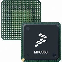
MPC855TCVR50D4 Freescale Semiconductor, MPC855TCVR50D4 Datasheet - Page 8

MPC855TCVR50D4
Manufacturer Part Number
MPC855TCVR50D4
Description
IC MPU POWERQUICC 50MHZ 357PBGA
Manufacturer
Freescale Semiconductor
Datasheets
1.MPC855TVR50D4.pdf
(15 pages)
2.MPC8555ECVTALF.pdf
(88 pages)
3.MPC855TCVR50D4.pdf
(80 pages)
Specifications of MPC855TCVR50D4
Processor Type
MPC8xx PowerQUICC 32-Bit
Speed
50MHz
Voltage
3.3V
Mounting Type
Surface Mount
Package / Case
357-PBGA
Processor Series
MPC8xx
Core
MPC8xx
Data Bus Width
32 bit
Maximum Clock Frequency
50 MHz
Operating Supply Voltage
2.5 V, 3.3 V
Maximum Operating Temperature
+ 95 C
Mounting Style
SMD/SMT
Minimum Operating Temperature
- 40 C
Family Name
MPC8xx
Device Core
PowerQUICC
Device Core Size
32b
Frequency (max)
50MHz
Instruction Set Architecture
RISC
Supply Voltage 1 (typ)
2.5/3.3V
Operating Supply Voltage (max)
3.465/3.6V
Operating Supply Voltage (min)
2/3.135V
Operating Temp Range
-40C to 95C
Operating Temperature Classification
Industrial
Mounting
Surface Mount
Pin Count
357
Package Type
BGA
Lead Free Status / RoHS Status
Lead free / RoHS Compliant
Features
-
Lead Free Status / Rohs Status
Lead free / RoHS Compliant
Available stocks
Company
Part Number
Manufacturer
Quantity
Price
Company:
Part Number:
MPC855TCVR50D4
Manufacturer:
FREESCAL
Quantity:
246
Company:
Part Number:
MPC855TCVR50D4
Manufacturer:
Freescale Semiconductor
Quantity:
10 000
Company:
Part Number:
MPC855TCVR50D4R2
Manufacturer:
Freescale Semiconductor
Quantity:
10 000
Freescale Semiconductor, Inc.
MPC855T Architecture Overview
branch prediction with conditional prefetch, but without conditional execution. The embedded core can
operate on 32-bit external operands with one bus cycle.
The integer unit supports 32- x 32-bit fixed-point general-purpose registers. It can execute one integer
instruction each clock cycle. Each element in the integer unit is clocked only when valid data is present in
the data queue ready for operation. This assures that the power consumption of the device is held to the
absolute minimum required to perform an operation.
The embedded core is integrated with MMUs as well as 4-Kbyte instruction and data caches. Each MMU
provides a 32-entry, fully-associative instruction and data TLB, with multiple page sizes of: 4 Kbytes, 16
Kbytes, 512 Kbytes, 256 Kbytes, and 8 Mbytes. It supports 16 virtual address spaces with 8 protection
groups. Three special registers are available as scratch registers to support software tablewalk and update.
The instruction cache is 4 Kbytes, two-way, set associative with physical addressing. It allows single-cycle
access on hit with no added latency for miss. It has four words per line, and supports burst linefill using least
recently used (LRU) replacement. The cache may be locked on a per-line basis for application-critical
routines.
The data cache is 4 Kbytes, two-way, set associative with physical addressing. It allows single-cycle access
on hit with one added clock latency for miss. It has four words per line, supporting burst linefill using LRU
replacement. The cache may be locked on a per-line basis for application-critical routines. The data cache
can be programmed to support copy-back or write-through via the MMU. The cache-inhibit mode can be
programmed per MMU page.
The embedded core with its instruction and data caches delivers approximately 106 MIPS at 80 MHz, using
Dhrystone 2.1, based on the assumption that it is issuing one instruction per cycle with a cache hit rate of
94%.
The embedded core provides a much improved debug interface that operates without causing any
degradation in the speed of user operations. This interface supports six watchpoint signals that are used to
detect software events. Internally the MPC855T has eight comparators, four of which operate on the
effective address on the address bus. The remaining four comparators are split, with two comparators
operating on the effective address on the data bus, and two comparators operating on the data on the data
bus. The embedded core can compare using =, , <, > conditions to generate watchpoints. Each watchpoint
can then generate a breakpoint that can be programmed to trigger in a programmable number of events.
1.2.2
Fast Ethernet Controller (FEC)
The Fast Ethernet controller on the MPC855T is compliant with the IEEE 802.3u specification for 10-Mbps
and 100-Mbps connectivity. Full-duplex 100-Mbps operation is supported at system clock rates of 50 MHz
and higher. A 33-MHz system clock supports 10-Mbps operation or half-duplex 100-Mbps operation.
The Fast Ethernet controller provides greatly reduced bus utilization through the use of bursting DMA.
Optimization of bus utilization allows the MPC855T to be used in systems with low-cost memories such as
synchronous DRAM.
Transmit and receive FIFOs further reduce bus utilization by localizing all collisions to the Fast Ethernet
controller. On the transmit side, a full collision window of transmit frame data is maintained in the FIFO,
eliminating the need for repeated DMA over the system bus in the event of a collision. On the receive side,
a full collision window of data is received before any receive data is transferred into system memory,
allowing the FIFO to be flushed in the event of a runt or collided frame, with no DMA activity. However,
external memory for data buffers and buffer descriptors is required; on-chip FIFOs are only designed to
compensate for collisions and for system bus latency.
8
MPC855T Communications Controller Technical Summary
MOTOROLA
For More Information On This Product,
Go to: www.freescale.com


