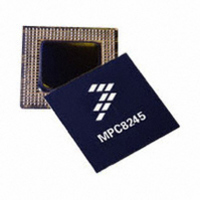
MPC8245LZU266D Freescale Semiconductor, MPC8245LZU266D Datasheet - Page 61

MPC8245LZU266D
Manufacturer Part Number
MPC8245LZU266D
Description
IC MPU 32BIT 266MHZ 352-TBGA
Manufacturer
Freescale Semiconductor
Series
PowerQUICC IIr
Datasheet
1.MPC8245LZU266D.pdf
(68 pages)
Specifications of MPC8245LZU266D
Processor Type
MPC82xx PowerQUICC II 32-bit
Speed
266MHz
Voltage
1.8V
Mounting Type
Surface Mount
Package / Case
352-TBGA
Core Size
32 Bit
Program Memory Size
32KB
Cpu Speed
266MHz
Embedded Interface Type
I2C
Digital Ic Case Style
TBGA
No. Of Pins
352
Supply Voltage Range
1.7V To 2.1V
Rohs Compliant
No
Lead Free Status / RoHS Status
Contains lead / RoHS non-compliant
Features
-
Available stocks
Company
Part Number
Manufacturer
Quantity
Price
Company:
Part Number:
MPC8245LZU266D
Manufacturer:
FREESCAL
Quantity:
237
Company:
Part Number:
MPC8245LZU266D
Manufacturer:
Freescale Semiconductor
Quantity:
10 000
Part Number:
MPC8245LZU266D
Manufacturer:
FREESCALE
Quantity:
20 000
Freescale Semiconductor
Revision
0.1
0.0
Date
—
—
Made V
Section 1.3, Table 2, Table 5, Table 9, Table 17, and Section 1.7.2.
Pin D17, formerly LAV
supplied internally. Eliminated all references to LAV
Previous Note 4 of Table 2 did not apply to the MPC8245 (MPC8240 document legacy). New Note 4
added in reference to maximum CPU speed at reduced V
Updated the Programmable Output Impedance of DEV_MEM_ADDR in Table 4 to 6 Ω to reflect
characterization data.
Updated Table 5 to reflect reduced power consumption when operating V
100 mV. Changed Notes 2, 3, and 4 to reflect V
= 1.8 V.
Updated Table 7 to reflect V
changed 250 MHz device column to 266 MHz; modified Note 1 eliminating VCO references; added
Note 2. Changed 250 MHz processor frequency offering to 266 MHz.
Changed Spec 12b for memory output valid time in
specification change to enable 133-MHz memory interface designs.
Updated Pinout Table 16 with the following changes:
Updated PLL Table 17 with the following changes for 133-MHz memory interface operation:
Added information to Section 1.7.8 in reference to CHKSTOP_IN and SRESET being unavailable in
extended ROM mode.
Initial release.
• Pin types for RCS0, RCS3/TRIG_OUT and DA[11:15] were erroneously listed as I/O, changed Pin
• Pin types for REQ4/DA4, RCS2/TRIG_IN, and PLL_CFG[0:4]/DA[10:6] were erroneously listed as
• Changed Pin D17 from LAV
• Notes 3, 5, and 7 contained references to the MPC8240 (MPC8240 document legacy); changed
• Previous Notes 13 and 14 did not apply to the MPC8245 (MPC8240 document legacy), these notes
• Added Note 3 to SDMA[1:0] signals about internal pull-up resistors during reset state.
• Reversed vector ordering for the PCI Interface Signals: C/BE[0:3] changed to C/BE[3:0], AD[0:31]
• Changed TEST1/DRDY signal on pin B20 to DRDY.
• Changed TEST2 signal on pin Y2 to RTC for performance monitor use.
• Added Ref. 9 (01001) and Ref. 17 (10111) details; removed these settings from Note 10 (reserved
• Enhanced range of Ref. 10 (10000).
• Updated Note 13, changed bits 16–20 erroneous information to correct bits 23–19.
• Added Notes 16 and 17.
Types to Output.
Input, changed Pin Types to I/O.
these references to MPC8245.
were deleted; moved Note 19 to become new Note 13; moved Note 20 to become new Note 14;
updated associated references.
changed to AD[31:0], GNT[0:3] changed to GNT[3:0], and REQ[0:3] changed to REQ[3:0]. The
package pin number orderings were also reversed meaning that pin functionality did NOT change.
For example, AD0 is still on signal C22, AD1 is still on signal D22,..., AD31 is still on signal V25. This
change was made to make the vectored PCI signals in this hardware specification consistent with
the PCI Local Bus Specification and the MPC8245 Integrated Processor Reference Manual vector
ordering.
settings list).
MPC8245 Integrated Processor Hardware Specifications, Rev. 10
DD
/AV
Table 19. Revision History Table (continued)
DD
/AV
DD
DD
2 = 1.8 V ± 100 mV information for 133-MHz memory interface operation to
(supply voltage for DLL), is a NC on the MPC8245 since the DLL voltage is
DD
/AV
DD
to No Connect; deleted Note 21 and references.
DD
/AV
Substantive Change(s)
DD
2 voltage level operating frequency dependencies;
DD
at 1.9 V. Changed Note 5 to represent V
DD
Table 11
; updated Section 1.7.1.
DD
from 5.5 ns to 4.5 ns; this is a key
voltage.
DD
Document Revision History
/AV
DD
/AV
DD
2 = 1.8 V ±
DD
= AV
DD
61


