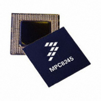
MPC8245LZU266D Freescale Semiconductor, MPC8245LZU266D Datasheet - Page 8

MPC8245LZU266D
Manufacturer Part Number
MPC8245LZU266D
Description
IC MPU 32BIT 266MHZ 352-TBGA
Manufacturer
Freescale Semiconductor
Series
PowerQUICC IIr
Datasheet
1.MPC8245LZU266D.pdf
(68 pages)
Specifications of MPC8245LZU266D
Processor Type
MPC82xx PowerQUICC II 32-bit
Speed
266MHz
Voltage
1.8V
Mounting Type
Surface Mount
Package / Case
352-TBGA
Core Size
32 Bit
Program Memory Size
32KB
Cpu Speed
266MHz
Embedded Interface Type
I2C
Digital Ic Case Style
TBGA
No. Of Pins
352
Supply Voltage Range
1.7V To 2.1V
Rohs Compliant
No
Lead Free Status / RoHS Status
Contains lead / RoHS non-compliant
Features
-
Available stocks
Company
Part Number
Manufacturer
Quantity
Price
Company:
Part Number:
MPC8245LZU266D
Manufacturer:
FREESCAL
Quantity:
237
Company:
Part Number:
MPC8245LZU266D
Manufacturer:
Freescale Semiconductor
Quantity:
10 000
Part Number:
MPC8245LZU266D
Manufacturer:
FREESCALE
Quantity:
20 000
Electrical and Thermal Characteristics
Figure 2
8
shows supply voltage sequencing and separation cautions.
Notes:
1. Numbers associated with waveform separations correspond to caution numbers listed in
2. See the Cautions section of
3. See
4. Refer to
5. HRST_CPU/HRST_CTRL must transition from a logic 0 to a logic 1 in less than one
6. PLL_CFG signals must be driven on reset and must be held for at least 25 clock cycles after the
SDRAM_SYNC_IN clock cycle for the device to be in the nonreset state.
negation of HRST_CTRL and HRST_CPU in order to be latched.
3.3 V
2.0 V
5 V
Table 8
0
Configuration Pins
Table 10
Figure 2. Supply Voltage Sequencing and Separation Cautions
for details on PLL relock and reset signal assertion timing requirements.
MPC8245 Integrated Processor Hardware Specifications, Rev. 10
HRST_CTRL
HRST_CPU,
Power Supply Ramp Up
for additional information on reset configuration pin setup timing requirements.
8
Reset
11
Table 2
11
V
Maximum Rise Time Must Be Less Than
DD
10
for details on this topic.
10
Stable
One External Memory Clock Cycle
2
7, 9
Clock Cycles Setup Time
See Note 1
Nine External Memory
Relock
100 µs
Time
PLL
3
External Memory
Clock Cycles
LV
OV
V
HRST_CTRL
Asserted 255
HRST_CPU,
DD
DD
DD
/AV
@ 5 V
/GV
4
DD
5
DD
/AV
/(LV
3
DD
DD
2
@ 3.3 V - - - -)
Freescale Semiconductor
PLL
VM = 1.4 V
Table
6
Time
2.


