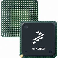
MPC860TVR50D4 Freescale Semiconductor, MPC860TVR50D4 Datasheet - Page 55

MPC860TVR50D4
Manufacturer Part Number
MPC860TVR50D4
Description
IC MPU POWERQUICC 50MHZ 357PBGA
Manufacturer
Freescale Semiconductor
Series
PowerQUICC Ir
Datasheet
1.MC860DECVR50D4R2.pdf
(80 pages)
Specifications of MPC860TVR50D4
Processor Type
MPC8xx PowerQUICC 32-Bit
Speed
50MHz
Voltage
3.3V
Mounting Type
Surface Mount
Package / Case
357-PBGA
Processor Series
MPC8xx
Core
MPC8xx
Data Bus Width
32 bit
Maximum Clock Frequency
50 MHz
Operating Supply Voltage
2.5 V, 3.3 V
Maximum Operating Temperature
+ 95 C
Mounting Style
SMD/SMT
Minimum Operating Temperature
0 C
Core Size
32 Bit
Program Memory Size
8KB
Cpu Speed
50MHz
Embedded Interface Type
Ethernet, I2C, SPI, UART
Digital Ic Case Style
BGA
No. Of Pins
357
Rohs Compliant
Yes
Lead Free Status / RoHS Status
Lead free / RoHS Compliant
Features
-
Lead Free Status / Rohs Status
Lead free / RoHS Compliant
Available stocks
Company
Part Number
Manufacturer
Quantity
Price
Company:
Part Number:
MPC860TVR50D4
Manufacturer:
Freescale Semiconductor
Quantity:
10 000
Company:
Part Number:
MPC860TVR50D4R2
Manufacturer:
Freescale Semiconductor
Quantity:
10 000
11.7
Table 20
1
2
Table 21
1
2
Freescale Semiconductor
Num
Num
100
101
102
103
104
105
106
107
108
The ratios SYNCCLK/RCLK1 and SYNCCLK/TCLK1 must be greater than or equal to 2.25/1.
Also applies to CD and CTS hold time when they are used as external sync signals.
100
102
103
104
105
106
107
108
The ratios SYNCCLK/RCLK1 and SYNCCLK/TCLK1 must be greater than or equal to 3/1.
Also applies to CD and CTS hold time when they are used as external sync signals.
RCLK1 and TCLK1 width high
RCLK1 and TCLK1 width low
RCLK1 and TCLK1 rise/fall time
TXD1 active delay (from TCLK1 falling edge)
RTS1 active/inactive delay (from TCLK1 falling edge)
CTS1 setup time to TCLK1 rising edge
RXD1 setup time to RCLK1 rising edge
RXD1 hold time from RCLK1 rising edge
CD1 setup Time to RCLK1 rising edge
RCLK1 and TCLK1 frequency
RCLK1 and TCLK1 rise/fall time
TXD1 active delay (from TCLK1 falling edge)
RTS1 active/inactive delay (from TCLK1 falling edge)
CTS1 setup time to TCLK1 rising edge
RXD1 setup time to RCLK1 rising edge
RXD1 hold time from RCLK1 rising edge
CD1 setup time to RCLK1 rising edge
provides the NMSI external clock timing.
provides the NMSI internal clock timing.
SCC in NMSI Mode Electrical Specifications
MPC860 PowerQUICC™ Family Hardware Specifications, Rev. 8
Characteristic
Characteristic
1
1
Table 20. NMSI External Clock Timing
Table 21. NMSI Internal Clock Timing
2
2
1/SYNCCLK + 5
1/SYNCCLK
0.00
5.00
5.00
0.00
5.00
5.00
Min
—
40.00
40.00
40.00
All Frequencies
0.00
0.00
0.00
0.00
Min
—
All Frequencies
CPM Electrical Characteristics
SYNCCLK/3
15.00
50.00
50.00
Max
30.00
30.00
Max
—
—
—
—
—
—
—
—
—
—
—
MHz
Unit
Unit
ns
ns
ns
ns
ns
ns
ns
ns
ns
ns
ns
ns
ns
ns
ns
ns
55


