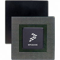
MPC8349EVVAJFB Freescale Semiconductor, MPC8349EVVAJFB Datasheet - Page 37

MPC8349EVVAJFB
Manufacturer Part Number
MPC8349EVVAJFB
Description
IC MPU POWERQUICC II 672-TBGA
Manufacturer
Freescale Semiconductor
Series
PowerQUICC II PROr
Datasheet
1.MPC8349EVVAJFB.pdf
(87 pages)
Specifications of MPC8349EVVAJFB
Processor Type
MPC83xx PowerQUICC II Pro 32-Bit
Speed
533MHz
Voltage
1.2V
Mounting Type
Surface Mount
Package / Case
672-TBGA
Processor Series
MPC8xxx
Core
e300
Data Bus Width
32 bit
Development Tools By Supplier
MPC8349E-MITXE
Maximum Clock Frequency
533 MHz
Maximum Operating Temperature
+ 105 C
Mounting Style
SMD/SMT
I/o Voltage
1.8 V, 2.5 V, 3.3 V
Minimum Operating Temperature
0 C
Core Size
32 Bit
Program Memory Size
64KB
Cpu Speed
533MHz
Embedded Interface Type
I2C, SPI, USB, UART
Digital Ic Case Style
TBGA
No. Of Pins
672
Rohs Compliant
Yes
For Use With
MPC8349E-MITX-GP - KIT REFERENCE PLATFORM MPC8349EMPC8349E-MITXE - BOARD REFERENCE FOR MPC8349MPC8349EA-MDS-PB - KIT MODULAR DEV SYSTEM MPC8349E
Lead Free Status / RoHS Status
Lead free / RoHS Compliant
Features
-
Lead Free Status / Rohs Status
Lead free / RoHS Compliant
Available stocks
Company
Part Number
Manufacturer
Quantity
Price
Company:
Part Number:
MPC8349EVVAJFB
Manufacturer:
Freescale Semiconductor
Quantity:
135
Company:
Part Number:
MPC8349EVVAJFB
Manufacturer:
FREESCALE
Quantity:
45
Company:
Part Number:
MPC8349EVVAJFB
Manufacturer:
Freescale Semiconductor
Quantity:
10 000
Part Number:
MPC8349EVVAJFB
Manufacturer:
FS
Quantity:
20 000
Figure 19
Freescale Semiconductor
Local bus cycle time
Input setup to local bus clock
Input hold from local bus clock
LALE output fall to LAD output transition (LATCH hold time)
LALE output fall to LAD output transition (LATCH hold time)
LALE output fall to LAD output transition (LATCH hold time)
Local bus clock to output valid
Local bus clock to output high impedance for LAD/LDP
Notes:
1. The symbols for timing specifications follow the pattern of t
2. All timings are in reference to the falling edge of LCLK0 (for all outputs and for LGTA and LUPWAIT inputs) or the rising edge
3. All signals are measured from OV
4. Input timings are measured at the pin.
5. t
6. t
7. t
8. For purposes of active/float timing measurements, the Hi-Z or off-state is defined to be when the total current delivered
9. DLL bypass mode is not recommended for use at frequencies above 66 MHz.
and t
for the input (I) to go invalid (X) with respect to the time the t
(1). Also, t
(O) going invalid (X) or output hold time.
of LCLK0 (for all other inputs).
signaling levels.
load on the LAD output pins.
the load on the LAD output pins.the
LAD output pins.
through the component pin is less than or equal to the leakage current specification.
LBOTOT1
LBOTOT2
LBOTOT3
(first two letters of functional block)(reference)(state)(signal)(state)
provides the AC test load for the local bus.
should be used when RCWH[LALE] is set and when the load on the LALE output pin is at least 10 pF less than the
should be used when RCWH[LALE] is not set and when the load on the LALE output pin is at least 10 pF less than
should be used when RCWH[LALE] is not set and when the load on the LALE output pin equals to the load on the
LBKHOX
MPC8349EA PowerQUICC II Pro Integrated Host Processor Hardware Specifications, Rev. 12
symbolizes local bus timing (LB) for the t
Table 39. Local Bus General Timing Parameters—DLL Bypass
Parameter
Output
DD
/2 of the rising/falling edge of LCLK0 to 0.4 × OV
Figure 19. Local Bus C Test Load
Z
0
= 50 Ω
for outputs. For example, t
(first two letters of functional block)(signal)(state)(reference)(state)
LBK
LBK
clock reference (K) to go high (H), with respect to the output
clock reference (K) goes high (H), in this case for clock one
Symbol
t
t
t
t
t
LBOTOT1
LBOTOT2
LBOTOT3
t
t
LBKHOZ
LBKLOV
LBIVKH
LBIXKH
t
LBK
R
1
L
= 50 Ω
Min
1.0
1.5
2.5
15
—
—
7
3
LBIXKH1
DD
OV
of the signal in question for 3.3 V
DD
symbolizes local bus timing (LB)
/2
Max
—
—
—
—
—
—
3
4
9
Unit
ns
ns
ns
ns
ns
ns
ns
ns
for inputs
Local Bus
Notes
3, 4
3, 4
2
5
6
7
3
8
37


