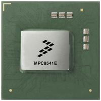
MPC8541EVTAPF Freescale Semiconductor, MPC8541EVTAPF Datasheet - Page 35

MPC8541EVTAPF
Manufacturer Part Number
MPC8541EVTAPF
Description
IC MPU POWERQUICC III 783-FCPBGA
Manufacturer
Freescale Semiconductor
Series
PowerQUICC IIIr
Specifications of MPC8541EVTAPF
Processor Type
MPC85xx PowerQUICC III 32-Bit
Speed
833MHz
Voltage
1.2V
Mounting Type
Surface Mount
Package / Case
783-FCPBGA
Core Size
32 Bit
Program Memory Size
64KB
Cpu Speed
833MHz
Digital Ic Case Style
BGA
No. Of Pins
783
Supply Voltage Range
1.14V To 1.26V
Rohs Compliant
Yes
Family Name
MPC85XX
Device Core
PowerQUICC III
Device Core Size
32b
Frequency (max)
833MHz
Instruction Set Architecture
RISC
Supply Voltage 1 (typ)
1.2V
Operating Supply Voltage (max)
1.26V
Operating Supply Voltage (min)
1.14V
Operating Temp Range
0C to 105C
Operating Temperature Classification
Commercial
Mounting
Surface Mount
Pin Count
783
Package Type
FCBGA
For Use With
MPC8548CDS - DEV TOOLS CDS FOR 8548CWH-PPC-8540N-VE - KIT EVAL SYSTEM MPC8540
Lead Free Status / RoHS Status
Lead free / RoHS Compliant
Features
-
Lead Free Status / Rohs Status
Compliant
Available stocks
Company
Part Number
Manufacturer
Quantity
Price
Company:
Part Number:
MPC8541EVTAPF
Manufacturer:
FREE
Quantity:
12
Company:
Part Number:
MPC8541EVTAPF
Manufacturer:
Freescale Semiconductor
Quantity:
10 000
Part Number:
MPC8541EVTAPF
Manufacturer:
FREESCALE
Quantity:
20 000
Company:
Part Number:
MPC8541EVTAPFF
Manufacturer:
FREESCAL
Quantity:
210
Notes:
1. The symbols used for timing specifications herein follow the pattern of t
2. All timings are in reference to LSYNC_IN for DLL enabled mode.
3. All signals are measured from OV
4. Input timings are measured at the pin.
5. For purposes of active/float timing measurements, the Hi-Z or off state is defined to be when the total current delivered
6. The value of t
7. Maximum possible clock skew between a clock LCLK[m] and a relative clock LCLK[n]. Skew measured between
8. Guaranteed by characterization.
9. Guaranteed by design.
Figure 16
Freescale Semiconductor
Local bus clock to address valid for LAD
Output hold from local bus clock (except
LAD/LDP and LALE)
Output hold from local bus clock for LAD/LDP
Local bus clock to output high Impedance
(except LAD/LDP and LALE)
Local bus clock to output high impedance for
LAD/LDP
for inputs and t
timing (LB) for the input (I) to go invalid (X) with respect to the time the t
clock one(1). Also, t
output (O) going invalid (X) or output hold time.
in question for 3.3-V signaling levels.
through the component pin is less than or equal to the leakage current specification.
bus buffer delays used as programmed at power-on reset with configuration pins LWE[0:1].
complementary signals at OV
MPC8541E PowerQUICC™ III Integrated Communications Processor Hardware Specification, Rev. 4.2
provides the AC test load for the local bus.
LBOTOT
Parameter
(First two letters of functional block)(reference)(state)(signal)(state)
Table 31. Local Bus General Timing Parameters—DLL Bypassed (continued)
LBKHOX
is defined as the sum of 1/2 or 1 ccb_clk cycle as programmed by LBCR[AHD], and the number of local
Output
symbolizes local bus timing (LB) for the t
DD
/2.
DD
/2 of the rising edge of local bus clock for DLL bypass mode to 0.4 × OV
Figure 16. Local Bus C Test Load
LWE[0:1] = 11 (default)
LWE[0:1] = 11 (default)
LWE[0:1] = 11 (default)
LWE[0:1] = 11 (default)
LWE[0:1] = 11 (default)
Z
Configuration
0
LWE[0:1] = 00
LWE[0:1] = 00
LWE[0:1] = 00
LWE[0:1] = 00
LWE[0:1] = 00
= 50 Ω
7
LBK
for outputs. For example, t
Symbol
(First two letters of functional block)(signal)(state) (reference)(state)
t
t
t
t
t
LBKLOV3
LBKLOX1
LBKLOX2
LBKLOZ1
LBKLOZ2
LBK
clock reference (K) to go high (H), with respect to the
R
clock reference (K) goes high (H), in this case for
L
= 50 Ω
1
–2.7
–1.8
–2.7
–1.8
Min
—
—
—
OV
DD
/2
LBIXKH1
Max
0.8
2.3
1.0
2.4
1.0
2.4
—
—
symbolizes local bus
Unit
ns
ns
ns
ns
ns
DD
of the signal
Local Bus
Notes
3
3
3
5
5
35


