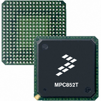
MPC852TVR100 Freescale Semiconductor, MPC852TVR100 Datasheet - Page 10

MPC852TVR100
Manufacturer Part Number
MPC852TVR100
Description
IC MPU POWERQUICC 100MHZ 256PBGA
Manufacturer
Freescale Semiconductor
Datasheet
1.MPC852TVR100.pdf
(80 pages)
Specifications of MPC852TVR100
Processor Type
MPC8xx PowerQUICC 32-Bit
Speed
100MHz
Voltage
1.8V
Mounting Type
Surface Mount
Package / Case
256-PBGA
Lead Free Status / RoHS Status
Contains lead / RoHS non-compliant
Features
-
Available stocks
Company
Part Number
Manufacturer
Quantity
Price
Company:
Part Number:
MPC852TVR100
Manufacturer:
MOT
Quantity:
12 388
Company:
Part Number:
MPC852TVR100
Manufacturer:
FREESCAL
Quantity:
364
Company:
Part Number:
MPC852TVR100
Manufacturer:
Freescale Semiconductor
Quantity:
10 000
Company:
Part Number:
MPC852TVR100A
Manufacturer:
MOTOROLA
Quantity:
490
Company:
Part Number:
MPC852TVR100A
Manufacturer:
Freescale Semiconductor
Quantity:
10 000
References
7.5 Experimental Determination
To determine the junction temperature of the device in the application after prototypes are available, the thermal
characterization parameter (Ψ
temperature at the top center of the package case using the following equation:
T
where:
The thermal characterization parameter is measured per JESD51-2 specification published by JEDEC using a
40-gauge type T thermocouple epoxied to the top center of the package case. The thermocouple should be positioned
so that the thermocouple junction rests on the package. A small amount of epoxy is placed over the thermocouple
junction and over about 1 mm of wire extending from the junction. The thermocouple wire is placed flat against the
package case to avoid measurement errors that cooling effects of the thermocouple wire cause.
8 References
Semiconductor Equipment and Materials International(415) 964-5111
805 East Middlefield Rd
Mountain View, CA 94043
MIL-SPEC and EIA/JESD (JEDEC) specifications800-854-7179 or
(Available from Global Engineering documents)303-397-7956
JEDEC Specifications http://www.jedec.org
1. C.E. Triplett and B. Joiner, “An Experimental Characterization of a 272 PBGA Within an Automotive Engine
Controller Module,” Proceedings of SemiTherm, San Diego, 1998, pp. 47-54.
2. B. Joiner and V. Adams, “Measurement and Simulation of Junction to Board Thermal Resistance and Its
Application in Thermal Modeling,” Proceedings of SemiTherm, San Diego, 1999, pp. 212-220.
9 Power Supply and Power Sequencing
This section provides design considerations for the MPC852T power supply. The MPC852T has a core voltage
(V
the MPC852T is supplied with 3.3 V across V
The signal PA[0:3], PA[8:11], PB15, PB[24:25]; PB[28:31], PC[4:7], PC[12:13], PC15] PD[3:15], TDI, TDO, TCK,
TRST, TMS, MII_TXEN, MII_MDIO are 5 V-tolerant. All inputs cannot be more than 2.5 V greater than V
addition, 5 V-tolerant pins can not exceed 5.5 V, and remaining input pins cannot exceed 3.465 V. This restriction
applies to power-on reset or power down and normal operation.
10
J
DDL
= T
T
) and PLL voltage (V
Ψ
T
P
+(Ψ
D
T
JT
= thermocouple temperature on top of package
= power dissipation in package
JT
= thermal characterization parameter
x P
D
)
DDSYN
JT
) can be used to determine the junction temperature with a measurement of the
) that operates at a lower voltage than the I/O voltage V
MPC852T Hardware Specifications, Rev. 3.1
DDH
and V
SS
(GND).
DDH
Freescale Semiconductor
. The I/O section of
DDH
. In


