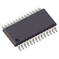
CS4272-DZZ Cirrus Logic Inc, CS4272-DZZ Datasheet

CS4272-DZZ
Specifications of CS4272-DZZ
Available stocks
Related parts for CS4272-DZZ
CS4272-DZZ Summary of contents
Page 1
... Microsoft Windows configuration of the board easy. The software communi- cates through the PC’s parallel port to configure the hardware so that all features of the CS4272 can be eval- Evaluation Board uated. The evaluation board may also be configured to accept external timing and data signals for operation in a user application during system development ...
Page 2
... TABLE OF CONTENTS 1. SYSTEM OVERVIEW ............................................................................................................... 4 1.1 CS4272 Stereo Audio CODEC .......................................................................................... 4 1.2 CS8406 Digital Audio Transmitter ...................................................................................... 4 1.3 CS8416 Digital Audio Receiver .......................................................................................... 4 1.4 Canned Oscillator .............................................................................................................. 5 1.5 Analog Input ....................................................................................................................... 5 1.6 Analog Outputs .................................................................................................................. 5 1.7 Stand-Alone Control ........................................................................................................... 7 1.8 PC Parallel Port Control ..................................................................................................... 7 1.9 External Control Headers ................................................................................................... 8 1.10 Power ............................................................................................................................... 8 1 ...
Page 3
... Figure 3. Advanced Window ......................................................................................................... 14 Figure 4. I²C Error Message.......................................................................................................... 14 Figure 5. Clock and Data Routing ................................................................................................. 15 Figure 6. Hierarchy, Schematic Sheet 1 ....................................................................................... 16 Figure 7. CS4272, Schematic Sheet 2.......................................................................................... 17 Figure 8. Analog Input, Schematic Sheet 3................................................................................... 18 Figure 9. Analog Output, Schematic Sheet 4................................................................................ 19 Figure 10. CS8416 S/PDIF Receiver, Schematic Sheet 5 ............................................................ 20 Figure 11 ...
Page 4
... The CDB4272 is able to operate the CS8406 in either master or slave mode. The serial audio input data for the CS8406 is received from the serial audio output of the CS4272. Using the GUI, the user may elect to supply the CS8406 with an external serial audio data source through a stake header (J17) ...
Page 5
... XLR connectors supply the CS4272 analog inputs through unity gain, AC-coupled differential circuits Vrms differential signal will drive the CS4272 inputs to full scale. The CDB4272 was designed for use with not only the CS4272, but also the CS421 with a simple change of assembly options. For this reason, the input buffer schematic shown in Figure 8 reflects only the configuration assembled on the CDB4272 ...
Page 6
The resistor designated by R2 (see Figure 1) can be adjusted to change the gain of the in- strumentation amp. The feedback resistors ‘R’ on the two sides of the instrumentation amp must be equal. Figure 1. Instrumentation Amplifier Configuration ...
Page 7
... PC Parallel Port Control A graphical user interface is included with the CDB4272 to allow easy manipulation of all reg- isters of the CS4272 and hardware configuration of the CDB4272. Connecting a cable to the DB-25 connector (J31) will enable the PC control port, automatically disabling switch S1 and its associated logic. ...
Page 8
... GUI. Also accessible from this header is a buffered version of the SDOUT signal from the CS4272, and a buffered input which, using S1 or the GUI, can be configured to drive the CS4272 SDIN pin. Care should be taken to ensure that the crystal (Y2) is removed when the board is configured to receive MCLK from this header ...
Page 9
... External data source for CS8406 SDIN 2 I/O for external SPI / I C control port signals (J32) and control signal header in/out selection (J34) XLR jacks for differential analog input signal to CS4272 RCA phono jacks for analog outputs Table 1. System Connections CDB4272 2 C control port signals and sys- ...
Page 10
... JUMPER / SWITCH PURPOSE M/S[1:0] Subclock Master/Slave Select (S1) MCLK[1:0] Master Clock Source Select (S1) Header/8416 CS4272 SDIN Source Select (S1) Coaxial/ Optical or Coaxial S/PDIF Optical Input Select (S1) I2S/LJ Digital Interface Format Select (S1) 128/256 Master Clock Speed Select (S1) M[1:0] CS4272 Speed Mode Select (S1) J11, J19 ...
Page 11
INITIAL BOARD SETUP 2.1 Power Supplies: 1) Verify that all power supplies are off before making connections. 2) Connect a +5.0 VDC power supply to the +5V (J1) red binding post. If correct configura- tion is other than the ...
Page 12
Board Operation connected, disconnect the PC parallel cable. 2) Set all positions LO, with the exception of M0 which should be set to HI. 3) Assert a reset by pressing the RESET button (S2). ...
Page 13
... The CS4271/2 Setup box allows configuration of the internal registers of the CS4272. Chang- es made within this box will be reflected immediately. When in I will read the registers of the CS4272 and update the CS4271/2 Setup box to match. Clicking the “Advanced...” button will launch a graphical register map of the CS4272. ...
Page 14
... I²C Mode No Acknowledge Error The control port of the CS4272 requires the presence of an MCLK signal for correct opera- tion. Because of this, if the board is set up to receive MCLK from a source that isn’t actively providing the signal acknowledge error may result. This means that the GUI is expecting an acknowledgement from the CS4272, but isn’ ...
Page 15
BLOCK DIAGRAM XTI XTO MCLK LRCK SCLK CDB4272 15 ...
Page 16
SCHEMATICS AND LAYOUT 16 CDB4272 ...
Page 17
CDB4272 17 ...
Page 18
CDB4272 ...
Page 19
CDB4272 19 ...
Page 20
CDB4272 ...
Page 21
CDB4272 21 ...
Page 22
CDB4272 ...
Page 23
CDB4272 23 ...
Page 24
CDB4272 ...
Page 25
CDB4272 25 ...
Page 26
CDB4272 ...
Page 27
CDB4272 27 ...
Page 28
CDB4272 ...
Page 29
APPENDIX Complete Analog Input Buffer Schematic CDB4272 29 ...


