TDA8024T/C1,118 NXP Semiconductors, TDA8024T/C1,118 Datasheet - Page 8
TDA8024T/C1,118
Manufacturer Part Number
TDA8024T/C1,118
Description
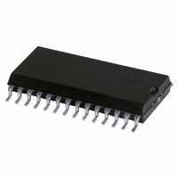
IC SMART CARD INTERFACE 28-SOIC
Manufacturer
NXP Semiconductors
Datasheet
1.TDA8024TTC1118.pdf
(29 pages)
Specifications of TDA8024T/C1,118
Package / Case
28-SOIC (7.5mm Width)
Controller Type
Smart Card Interface
Interface
Analog
Voltage - Supply
2.7 V ~ 6.5 V
Current - Supply
1.5mA
Operating Temperature
-25°C ~ 85°C
Mounting Type
Surface Mount
Maximum Operating Temperature
+ 85 C
Minimum Operating Temperature
- 25 C
Mounting Style
SMD/SMT
Lead Free Status / RoHS Status
Lead free / RoHS Compliant
Lead Free Status / RoHS Status
Lead free / RoHS Compliant, Lead free / RoHS Compliant
Other names
935271342118
TDA8024TD-T
TDA8024TD-T
TDA8024TD-T
TDA8024TD-T
Available stocks
Company
Part Number
Manufacturer
Quantity
Price

Part Number:
TDA8024T/C1,118
Manufacturer:
NXP/恩智浦
Quantity:
20 000


Philips Semiconductors
8
Throughout this document it is assumed that the reader is
familiar with ISO7816 terminology.
8.1
The supply pins for the IC are V
be in the range of 2.7 to 6.5 V. All signals interfacing with
the system controller are referred to V
should also supply the system controller. All card reader
contacts remain inactive during power-on or power-off.
The internal circuits are maintained in the reset state until
V
internal Power-on reset pulse, t
falls below V
is performed.
A DC/DC converter is incorporated to generate the
5 or 3 V card supply voltage (V
should be supplied separately by V
the possibility of large transient currents, the two 100 nF
capacitors of the DC/DC converter should be located as
near as possible to the IC and have an ESR less than
100 m .
The DC/DC converter functions as a voltage doubler or a
voltage follower according to the respective values of V
and V
100 mV).
2004 July 12
handbook, full pagewidth
DD
IC card interface
FUNCTIONAL DESCRIPTION
reaches V
DDP
(internal signal)
Power supply
(both have thresholds with a hysteresis of
ALARM
th2
V DD
th2
, an automatic deactivation of the contacts
+ V
hys2
and for the duration of the
power-on
CC
W
DD
). The DC/DC converter
(see Fig.5). When V
DDP
and GND. V
t w
DD
and PGND. Due to
, therefore V
Fig.5 Voltage supervisor.
DD
should
DD
supply dropout
DD
CC
8
The DC/DC converter function changes as follows:
Supply voltages V
any sequence.
After powering the device, OFF remains LOW until
CMDVCC is set HIGH.
During power off, OFF falls LOW when V
falling threshold voltage.
8.2
8.2.1
The voltage supervisor surveys the V
reset pulse of approximately 8 ms (t
keep the IC inactive during power-on or power-off of the
V
As long as V
inactive whatever the levels on the command lines. This
state also lasts for the duration of t
a level higher than V
When V
contacts is performed.
t w
DD
V
V
V
V
CC
CC
CC
CC
supply (see Fig.5).
= 5 V and V
= 5 V and V
= 3 V and V
= 3 V and V
Voltage supervisor
DD
W
(
OR WITH
falls below V
ITHOUT EXTERNAL DIVIDER ON PIN
DD
is less than V
DD
TDA8024AT)
DDP
DDP
DDP
DDP
th2
and V
> 5.8 V; voltage follower
< 5.7 V; voltage doubler
> 4.1 V; voltage follower
< 4.0 V; voltage doubler.
th2
+ V
, a deactivation sequence of the
DDP
hys2
power-off
th2
.
may be applied to the IC in
+ V
W
MDB053
W
after V
hys2
Product specification
DD
) is used internally to
, the IC remains
V th2 V hys2
V th2
supply. A defined
TDA8024
DD
DD
PORADJ
is below the
has reached
Related parts for TDA8024T/C1,118
Image
Part Number
Description
Manufacturer
Datasheet
Request
R

Part Number:
Description:
Manufacturer:
NXP Semiconductors
Datasheet:

Part Number:
Description:
IC SMART CARD INTERFACE 28-SOIC
Manufacturer:
NXP Semiconductors
Datasheet:
Part Number:
Description:
NXP Semiconductors designed the LPC2420/2460 microcontroller around a 16-bit/32-bitARM7TDMI-S CPU core with real-time debug interfaces that include both JTAG andembedded trace
Manufacturer:
NXP Semiconductors
Datasheet:

Part Number:
Description:
NXP Semiconductors designed the LPC2458 microcontroller around a 16-bit/32-bitARM7TDMI-S CPU core with real-time debug interfaces that include both JTAG andembedded trace
Manufacturer:
NXP Semiconductors
Datasheet:
Part Number:
Description:
NXP Semiconductors designed the LPC2468 microcontroller around a 16-bit/32-bitARM7TDMI-S CPU core with real-time debug interfaces that include both JTAG andembedded trace
Manufacturer:
NXP Semiconductors
Datasheet:
Part Number:
Description:
NXP Semiconductors designed the LPC2470 microcontroller, powered by theARM7TDMI-S core, to be a highly integrated microcontroller for a wide range ofapplications that require advanced communications and high quality graphic displays
Manufacturer:
NXP Semiconductors
Datasheet:
Part Number:
Description:
NXP Semiconductors designed the LPC2478 microcontroller, powered by theARM7TDMI-S core, to be a highly integrated microcontroller for a wide range ofapplications that require advanced communications and high quality graphic displays
Manufacturer:
NXP Semiconductors
Datasheet:
Part Number:
Description:
The Philips Semiconductors XA (eXtended Architecture) family of 16-bit single-chip microcontrollers is powerful enough to easily handle the requirements of high performance embedded applications, yet inexpensive enough to compete in the market for hi
Manufacturer:
NXP Semiconductors
Datasheet:
Part Number:
Description:
The XA-S3 device is a member of Philips Semiconductors? XA(eXtended Architecture) family of high performance 16-bitsingle-chip microcontrollers
Manufacturer:
NXP Semiconductors
Datasheet:

Part Number:
Description:
The NXP BlueStreak LH75401/LH75411 family consists of two low-cost 16/32-bit System-on-Chip (SoC) devices
Manufacturer:
NXP Semiconductors
Datasheet:
Part Number:
Description:
The NXP LPC3130/3131 combine an 180 MHz ARM926EJ-S CPU core, high-speed USB2
Manufacturer:
NXP Semiconductors
Datasheet:
Part Number:
Description:
The NXP LPC3141 combine a 270 MHz ARM926EJ-S CPU core, High-speed USB 2
Manufacturer:
NXP Semiconductors
Part Number:
Description:
The NXP LPC3143 combine a 270 MHz ARM926EJ-S CPU core, High-speed USB 2
Manufacturer:
NXP Semiconductors