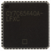
CY7C65640A-LFXC Cypress Semiconductor Corp, CY7C65640A-LFXC Datasheet - Page 20

CY7C65640A-LFXC
Manufacturer Part Number
CY7C65640A-LFXC
Description
IC USB HUB CONTROLLER HS 56VQFN
Manufacturer
Cypress Semiconductor Corp
Series
TetraHub™r
Specifications of CY7C65640A-LFXC
Controller Type
USB Hub
Interface
SPI Serial
Voltage - Supply
3.15 V ~ 3.45 V
Operating Temperature
0°C ~ 70°C
Mounting Type
Surface Mount
Package / Case
56-VQFN Exposed Pad, 56-HVQFN, 56-SQFN, 56-DHVQFN
Current - Supply
260mA
Operating Supply Voltage (typ)
3.3V
Operating Supply Voltage (min)
3.15V
Operating Supply Voltage (max)
3.45V
Operating Temp Range
0C to 70C
Operating Temperature Classification
Commercial
Mounting
Surface Mount
Pin Count
56
Lead Free Status / RoHS Status
Lead free / RoHS Compliant
For Use With
CY4602 - KIT USB 4-PORT HUB REF DESIGN
Lead Free Status / RoHS Status
Compliant, Lead free / RoHS Compliant
Other names
428-1805
CY7C65640A-LFXC
CY7C65640A-LFXC
Available stocks
Company
Part Number
Manufacturer
Quantity
Price
Company:
Part Number:
CY7C65640A-LFXC
Manufacturer:
CYPRESS
Quantity:
250
Part Number:
CY7C65640A-LFXC
Manufacturer:
CYPRESS/赛普拉斯
Quantity:
20 000
Note. The bottom metal pad size varies by product due to die
size variable. If metal pad design or dimension are critical with
your board designs, please contact a Cypress Sales office to get
the specific outline option.
Quad Flat Package No Leads (QFN) Package Design
Notes
The QFN (Quad Flatpack No Leads), being a lead free package,
the electrical contact of the part to the Printed Circuit Board
(PCB) is made by soldering the lands on the bottom surface of
the package to the PCB. Hence special attention is required to
the heat transfer area below the package to provide a good
thermal bond to the circuit board. A Copper (Cu) fill should be
designed into the PCB as a thermal pad under the package. Heat
is transferred from the TetraHub through the device’s metal
paddle on the bottom side of the package. Heat from here is
conducted to the PCB at the thermal pad. It is then conducted
from the thermal pad to the PCB inner ground plane by a 5 x 5
array of via. A via is a plated through-hole in the PCB with a
finished diameter of 13 mil. The QFN’s metal die paddle must be
soldered to the PCB’s thermal pad. Solder mask is placed on the
board top side over each via to resist solder flow into the via. The
Document #: 38-08019 Rev. *J
Figure 8. 56-Pin Sawn QFN (8X8X0.90 MM)
mask on the top side also minimizes outgassing during the solder
reflow process.
Please follow the layout guidelines provided in the PCB layout
files accompanied with the CY4602 TetraHub Reference Design
Kit. The information in this section was derived from the original
application note by the package vendor. For further information
on this package design please refer to the application note
“Surface Mount Assembly of AMKOR’s MicroLeadFrame (MLF)
Technology”. This application note can be downloaded from
AMKOR’s website from the following URL
http://www.amkor.com/products/notes_papers/MLF_AppNote_
0301.pdf.
This application note provides detailed information on board
mounting guidelines, soldering flow, rework process, etc.
Figure 9
package. The cross section is of only one via. The solder Paste
template needs to be designed to allow at least 50% solder
coverage. The thickness of the solder paste template should be
5 mil. It is recommended that “No Clean”, type 3 solder paste is
used for mounting the part. Nitrogen purge is recommended
during reflow.
below displays a cross-sectional area underneath the
51-85187 *C
CY7C65640A
Page 20 of 23
[+] Feedback


