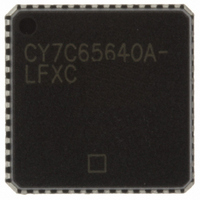
CY7C65640A-LFXC Cypress Semiconductor Corp, CY7C65640A-LFXC Datasheet - Page 6

CY7C65640A-LFXC
Manufacturer Part Number
CY7C65640A-LFXC
Description
IC USB HUB CONTROLLER HS 56VQFN
Manufacturer
Cypress Semiconductor Corp
Series
TetraHub™r
Specifications of CY7C65640A-LFXC
Controller Type
USB Hub
Interface
SPI Serial
Voltage - Supply
3.15 V ~ 3.45 V
Operating Temperature
0°C ~ 70°C
Mounting Type
Surface Mount
Package / Case
56-VQFN Exposed Pad, 56-HVQFN, 56-SQFN, 56-DHVQFN
Current - Supply
260mA
Operating Supply Voltage (typ)
3.3V
Operating Supply Voltage (min)
3.15V
Operating Supply Voltage (max)
3.45V
Operating Temp Range
0C to 70C
Operating Temperature Classification
Commercial
Mounting
Surface Mount
Pin Count
56
Lead Free Status / RoHS Status
Lead free / RoHS Compliant
For Use With
CY4602 - KIT USB 4-PORT HUB REF DESIGN
Lead Free Status / RoHS Status
Compliant, Lead free / RoHS Compliant
Other names
428-1805
CY7C65640A-LFXC
CY7C65640A-LFXC
Available stocks
Company
Part Number
Manufacturer
Quantity
Price
Company:
Part Number:
CY7C65640A-LFXC
Manufacturer:
CYPRESS
Quantity:
250
Part Number:
CY7C65640A-LFXC
Manufacturer:
CYPRESS/赛普拉斯
Quantity:
20 000
Table 0-1. CY7C65640APin Assignments
Document #: 38-08019 Rev. *J
SPI INTERFACE
UPSTREAM PORT
Pin
11
15
19
23
27
33
39
45
55
12
16
20
24
28
34
40
47
50
56
21
22
46
26
25
48
49
17
18
3
7
4
8
BUSPOWER
SPI_SCK
RESET#
SPI_CS
SPI_SD
XOUT
Name
GND
GND
GND
GND
GND
GND
GND
GND
GND
GND
GND
GND
VCC
VCC
VCC
VCC
VCC
VCC
VCC
VCC
VCC
VCC
VCC
XIN
D–
D+
Output
Power
Power
Power
Power
Power
Power
Power
Power
Power
Power
Power
Power
Power
Power
Power
Power
Power
Power
Power
Power
Power
Power
Power
Type
Input
Input
Input
I/O/Z
I/O/Z
I/O/Z
O
O
Default
N/A
N/A
N/A
N/A
N/A
N/A
N/A
N/A
N/A
N/A
N/A
N/A
N/A
N/A
N/A
N/A
N/A
N/A
N/A
N/A
N/A
N/A
N/A
N/A
N/A
N/A
N/A
O
O
Z
Z
Z
Description
V
V
V
V
V
V
V
V
V
V
V
GND. Connect to Ground with as short a path as possible.
GND. Connect to Ground with as short a path as possible.
GND. Connect to Ground with as short a path as possible.
GND. Connect to Ground with as short a path as possible.
GND. Connect to Ground with as short a path as possible.
GND. Connect to Ground with as short a path as possible.
GND. Connect to Ground with as short a path as possible.
GND. Connect to Ground with as short a path as possible.
GND. Connect to Ground with as short a path as possible.
GND. Connect to Ground with as short a path as possible.
GND. Connect to Ground with as short a path as possible.
GND. Connect to Ground with as short a path as possible.
24-MHz Crystal IN or External Clock Input.
24-MHz Crystal OUT.
Active LOW Reset. This pin resets the entire chip. It is normally tied to V
through a 100K resistor, and to GND through a 0.1-µF capacitor. Other than this,
no other special power-up procedure is required.
VBUS. Connect to the VBUS pin of the upstream connector. This signal indicates
to the hub that it is in a powered state, and may enable the D+ pull-up resistor
to indicate a connection. (The hub will do so after the external EEPROM is read,
unless it is put into a high speedhigh speedhigh speed mode by the upstream
hub). The hub can not be bus powered, and the VBUS signal must not be used
as a power source.
SPI Chip Select. Connect to CS pin of the EEPROM.
SPI Clock. Connect to EEPROM SCK pin.
SPI Dataline Connect to GND with 15-KΩ resistor and to the Data I/O pins of
the EEPROM.
Upstream D– Signal.
Upstream D+ Signal.
CC
CC
CC
CC
CC
CC
CC
CC
CC
CC
CC
. This signal provides power to the chip.
. This signal provides power to the chip.
. This signal provides power to the chip.
. This signal provides power to the chip.
. This signal provides power to the chip.
. This signal provides power to the chip.
. This signal provides power to the chip.
. This signal provides power to the chip.
. This signal provides power to the chip.
. This signal provides power to the chip.
. This signal provides power to the chip.
CY7C65640A
Page 6 of 23
CC
[+] Feedback


