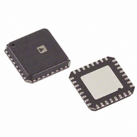
AD9913BCPZ Analog Devices Inc, AD9913BCPZ Datasheet - Page 23

AD9913BCPZ
Manufacturer Part Number
AD9913BCPZ
Description
IC DDS 10BIT DAC 250MSPS 32LFCSP
Manufacturer
Analog Devices Inc
Datasheet
1.AD9913BCPZ.pdf
(32 pages)
Specifications of AD9913BCPZ
Resolution (bits)
10 b
Master Fclk
250MHz
Tuning Word Width (bits)
32 b
Voltage - Supply
1.8 V
Operating Temperature
-40°C ~ 85°C
Mounting Type
Surface Mount
Package / Case
32-LFCSP
Ic Function
Direct Digital Synthesizer
Supply Voltage Range
1.7V To 1.9V
Operating Temperature Range
-40°C To +85°C
Digital Ic Case Style
LFCSP
No. Of Pins
32
Msl
MSL 3 - 168 Hours
Lead Free Status / RoHS Status
Lead free / RoHS Compliant
For Use With
AD9913/PCBZ - BOARD EVAL FOR AD9913
Lead Free Status / RoHS Status
Lead free / RoHS Compliant, Lead free / RoHS Compliant
Available stocks
Company
Part Number
Manufacturer
Quantity
Price
Company:
Part Number:
AD9913BCPZ
Manufacturer:
AD
Quantity:
319
Part Number:
AD9913BCPZ
Manufacturer:
ADI/亚德诺
Quantity:
20 000
Instruction Byte
The instruction byte contains the following information as
shown in the instruction byte bit map.
Instruction Byte Information Bit Map
MSB
D7
R/W
R/ W —Bit 7 of the instruction byte determines whether a read
or write data transfer occurs after the instruction byte write.
Logic high indicates read operation. Logic 0 indicates a write
operation.
X, X—Bit 6 and Bit 5 of the instruction byte are don’t care.
A4, A3, A2, A1, A0—Bit 4, Bit 3, Bit 2, Bit 1, and Bit 0 of the
instruction byte determine which register is accessed during the
data transfer portion of the communications cycle.
Serial Interface Port Pin Description
SCLK—Serial Port Clock
The serial clock pin is used to synchronize data to and from the
AD9913 and to run the internal state machines.
CS —Chip Select
Active low input that allows more than one device on the same
serial communications line. The SDIO pin goes to a high
impedance state when this input is high. If driven high during
any communications cycle, that cycle is suspended until chip
select is reactivated low. Chip select can be tied low in systems
that maintain control of SCLK.
SDIO—Serial Data I/O.
Data is always written into and read from the AD9913 on
this pin.
MSB/LSB Transfers
The AD9913 serial port can support both most significant bit
(MSB) first or least significant bit (LSB) first data formats. This
functionality is controlled by the CFR1 [23]. The default value
is MSB first. The instruction byte must be written in the format
indicated by Control Register 0x00 Bit 8. That is, if the AD9913
is in LSB first mode, the instruction byte must be written from
least significant bit to most significant bit.
D6
X
D5
X
D4
A4
D3
A3
D2
A2
D1
A1
LSB
D0
A0
Rev. A | Page 23 of 32
For MSB first operation, the serial port controller generates the
most significant byte (of the specified register) address first
followed by the next less significant byte addresses until the I/O
operation is complete. All data written to (read from) the
AD9913 must be in MSB first order.
If the LSB mode is active, the serial port controller generates the
least significant byte address first followed by the next greater
significant byte addresses until the I/O operation is complete.
All data written to (read from) the AD9913 must be in LSB
first order.
Notes on Serial Port Operation
The LSB first bit resides in CFR1 [23]. Note that the
configuration changes immediately upon writing to the byte
containing the LSB first bit. Therefore, care must be taken to
compensate for this new configuration for the remainder of the
current communication cycle.
Reading profile registers requires that the external profile select
pins (PS[2:0]) be configured to select the corresponding
register.
PARALLEL I/O PROGRAMMING
Parallel Port Interface Pin Description
CS —Chip Select
An active low on this pin indicates that a read/write operation is
about to be performed. If this pin goes high during an access,
the parallel port is reset to its initial condition.
R/ W —Read/Write
A high on Pin 29 combined with CS active low indicates a read
operation. A low on this pin indicates a write operation.
PCLK—Parallel Port Clock
The parallel clock pin is used to synchronize data to and from
the AD9913 and to run the internal state machines.
ADDR/DATA [7:0]
The 8-bit address/data bus. It works in a bidirectional fashion to
support both read and write operations.
Notes on Parallel Port Operation
Each operation works in a 3-PCLK cycle with the first clock
cycle for addressing, the second for reading or writing, and the
third for re-initialization. In parallel port operation, each byte is
programmed individually.
AD9913


