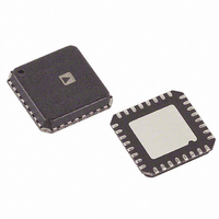
AD9913BCPZ Analog Devices Inc, AD9913BCPZ Datasheet - Page 24

AD9913BCPZ
Manufacturer Part Number
AD9913BCPZ
Description
IC DDS 10BIT DAC 250MSPS 32LFCSP
Manufacturer
Analog Devices Inc
Datasheet
1.AD9913BCPZ.pdf
(32 pages)
Specifications of AD9913BCPZ
Resolution (bits)
10 b
Master Fclk
250MHz
Tuning Word Width (bits)
32 b
Voltage - Supply
1.8 V
Operating Temperature
-40°C ~ 85°C
Mounting Type
Surface Mount
Package / Case
32-LFCSP
Ic Function
Direct Digital Synthesizer
Supply Voltage Range
1.7V To 1.9V
Operating Temperature Range
-40°C To +85°C
Digital Ic Case Style
LFCSP
No. Of Pins
32
Msl
MSL 3 - 168 Hours
Lead Free Status / RoHS Status
Lead free / RoHS Compliant
For Use With
AD9913/PCBZ - BOARD EVAL FOR AD9913
Lead Free Status / RoHS Status
Lead free / RoHS Compliant, Lead free / RoHS Compliant
Available stocks
Company
Part Number
Manufacturer
Quantity
Price
Company:
Part Number:
AD9913BCPZ
Manufacturer:
AD
Quantity:
319
Part Number:
AD9913BCPZ
Manufacturer:
ADI/亚德诺
Quantity:
20 000
AD9913
Data Read Operation
A typical read operation follows the steps shown in Figure 33.
1.
2.
3.
4.
5.
Data Write Operation
Write operations work in a similar fashion as read operations
except that the user drives the bus for both PCLK cycles. A
typical write access follows the steps shown in Figure 34.
The user supplies PCLK, CS , R/ W , and the parallel address
of the register using the address pins (ADR0 through
ADR7) for the read operation.
CS , R/ W , and the address lines must meet the setup and
hold times relative to the 1
The user releases the bus to read.
The AD9913 drives data onto the bus after the second
PCLK rising edge.
CS must meet the set up and hold times to the 3
rising edge.
ADDR/DATA
ADDR/DATA
PCLK
PCLK
R/W
R/W
CS
CS
t
3ns
ASU
t
3ns
ASU
ADDR0
ADDR0
0.3ns
0.3ns
t
t
st
AHD
AHD
PCLK rising edge.
t
3ns
DSU
DATA0
t
DVLD
8ns
0.3ns
t
DATA0
DHD
t
3ns
t
CSU
3ns
CSU
0.3ns
t
0.3ns
CHD
t
CHD
rd
Figure 33. Parallel Port Read Timing
Figure 34. Parallel Port Write Timing
PCLK
ADDR1
ADDR1
Rev. A | Page 24 of 32
DATA1
WRITE OPERATION
READ OPERATION
DATA1
1.
2.
3.
4.
5.
The user supplies the PCLK, CS , R/ W , and the parallel
address of the register and using the address pins
(ADR0/D0 through ADR7/D7).
CS , R/ W , and the address lines must meet the set up and
hold times relative to the 1
Data lines must meet the set up and hold times relative to
the 2
CS must meet the set up and hold times relative to the 3
PCK rising edge.
The IO_UPDATE is not shown in Figure 34. The
IO_UPDATE transfers the contents from a write sequence
to the active register. See the Register Update (I/O Update)
section.
nd
PCLK rising edge.
st
PCLK rising edge.
rd


