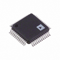
AD9954YSVZ Analog Devices Inc, AD9954YSVZ Datasheet - Page 19

AD9954YSVZ
Manufacturer Part Number
AD9954YSVZ
Description
IC DDS DAC 14BIT 1.8V 48-TQFP
Manufacturer
Analog Devices Inc
Datasheet
1.AD9954YSVZ-REEL7.pdf
(40 pages)
Specifications of AD9954YSVZ
Resolution (bits)
14 b
Master Fclk
400MHz
Tuning Word Width (bits)
32 b
Voltage - Supply
1.71 V ~ 1.96 V
Operating Temperature
-40°C ~ 105°C
Mounting Type
Surface Mount
Package / Case
48-TQFP Exposed Pad, 48-eTQFP, 48-HTQFP, 48-VQFP
Data Rate
25Mbps
Rf Ic Case Style
TQFP
No. Of Pins
48
Supply Voltage Range
1.71V To 1.89V, 3.135V To 3.465V
Operating Temperature Range
-40°C To +105°C
Msl
MSL 3 - 168 Hours
Termination Type
SMD
Rohs Compliant
Yes
Filter Terminals
SMD
Lead Free Status / RoHS Status
Lead free / RoHS Compliant
For Use With
AD9954/PCBZ - BOARD EVAL FOR 9954
Lead Free Status / RoHS Status
Lead free / RoHS Compliant, Lead free / RoHS Compliant
Available stocks
Company
Part Number
Manufacturer
Quantity
Price
Company:
Part Number:
AD9954YSVZ
Manufacturer:
ADI
Quantity:
210
Company:
Part Number:
AD9954YSVZ
Manufacturer:
Analog Devices Inc
Quantity:
10 000
Part Number:
AD9954YSVZ
Manufacturer:
ADI/亚德诺
Quantity:
20 000
Company:
Part Number:
AD9954YSVZ-REEL7
Manufacturer:
UBR
Quantity:
6 000
Company:
Part Number:
AD9954YSVZ-REEL7
Manufacturer:
Analog Devices Inc
Quantity:
10 000
Linear Sweep No-Dwell Feature
See CFR1<2> in the register maps (see Table 12 and Table 13)
for general details of the no-dwell mode. Figure 22 depicts the
linear sweep mode operation when the linear sweep no-dwell
bit is set. The Label A points indicate where a rising edge on
PS0 is detected; the Label B points indicate where the AD9954
has determined f
automatically returns to the starting frequency. Note that in this
mode, only sweeps from FTW0 to FTW1 using the positive
linear sweep control word are supported. Toggling PS0 from 1
to 0 neither initiates a falling sweep when the no-dwell bit is set,
nor interrupts a positive sweep already underway.
OUT
FTW1
FTW0
FTW1
FTW0
has reached the terminal frequency and
f
f
OUT
OUT
SINGLE-TONE
SINGLE-TONE
MODE
MODE
PS<0> = 0
PS<0> = 0
AT POINT A: LOAD RISING RAMP RATE REGISTER, APPLY RISING DFTW.
AT POINT B: LOAD FALLING RAMP RATE REGISTER, APPLY FALLING DFTW.
Figure 22. Linear Sweep Using No-Dwell Frequency Plan
A
A
PS<0> = 1 PS<0> = 0
Figure 21. Linear Sweep Frequency Plan
LINEAR SWEEP MODE ENABLE–NO DWELL BIT SET
LINEAR SWEEP MODE
PS<0> = 1
B
Rev. B | Page 19 of 40
A
PS<0> = 1
Resetting the Ramp Rate Timer
The ramp timer can be reset before reaching a count of 1 by
three methods.
Method one is by changing the PS0 input pin. When the PS0
input pin toggles from 0 to 1, the RSRRW value is loaded into
the ramp rate timer, which then proceeds to countdown as
normal. When the PS0 input pin toggles from 0 to 1, the falling
sweep ramp rate word (FSRRW) value is loaded into the ramp
rate timer, which then proceeds to countdown as normal.
The second method uses the LOAD SRR @ I/O UD bit
(CFR1<15>), see Table 12 for details.
B
B
PS<0> = 0
PS<0> = 0
A
PS<0> = 1
B
TIME
TIME
AD9954


