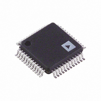
AD9954YSVZ Analog Devices Inc, AD9954YSVZ Datasheet - Page 23

AD9954YSVZ
Manufacturer Part Number
AD9954YSVZ
Description
IC DDS DAC 14BIT 1.8V 48-TQFP
Manufacturer
Analog Devices Inc
Datasheet
1.AD9954YSVZ-REEL7.pdf
(40 pages)
Specifications of AD9954YSVZ
Resolution (bits)
14 b
Master Fclk
400MHz
Tuning Word Width (bits)
32 b
Voltage - Supply
1.71 V ~ 1.96 V
Operating Temperature
-40°C ~ 105°C
Mounting Type
Surface Mount
Package / Case
48-TQFP Exposed Pad, 48-eTQFP, 48-HTQFP, 48-VQFP
Data Rate
25Mbps
Rf Ic Case Style
TQFP
No. Of Pins
48
Supply Voltage Range
1.71V To 1.89V, 3.135V To 3.465V
Operating Temperature Range
-40°C To +105°C
Msl
MSL 3 - 168 Hours
Termination Type
SMD
Rohs Compliant
Yes
Filter Terminals
SMD
Lead Free Status / RoHS Status
Lead free / RoHS Compliant
For Use With
AD9954/PCBZ - BOARD EVAL FOR 9954
Lead Free Status / RoHS Status
Lead free / RoHS Compliant, Lead free / RoHS Compliant
Available stocks
Company
Part Number
Manufacturer
Quantity
Price
Company:
Part Number:
AD9954YSVZ
Manufacturer:
ADI
Quantity:
210
Company:
Part Number:
AD9954YSVZ
Manufacturer:
Analog Devices Inc
Quantity:
10 000
Part Number:
AD9954YSVZ
Manufacturer:
ADI/亚德诺
Quantity:
20 000
Company:
Part Number:
AD9954YSVZ-REEL7
Manufacturer:
UBR
Quantity:
6 000
Company:
Part Number:
AD9954YSVZ-REEL7
Manufacturer:
Analog Devices Inc
Quantity:
10 000
Serial I/O Port
The AD9954 serial port is a flexible, synchronous, serial
communications port that easily interfaces to many industry-
standard microcontrollers and microprocessors. The serial I/O port
is compatible with most synchronous transfer formats, including
both the Motorola 6905/11 SPI® and Intel® 8051 SSR protocols.
The interface accesses all registers that configure the AD9954. MSB
first and LSB first transfer formats are supported. In addition, the
AD9954’s serial interface port can be configured as a single pin I/O
(SDIO), which allows a 2-wire interface, or two unidirectional pins
for in/out (SDIO/SDO), which enables a 3-wire interface. Two
optional pins, IOSYNC and CS , provide further flexibility for
system design with the AD9954.
SERIAL PORT OPERATION
With the AD9954, the instruction byte specifies read/write
operation and register address. Serial operations on the AD9954
only occur at the register level, they do not occur on the byte
level. For the AD9954, the serial port controller recognizes the
instruction byte register address and automatically generates the
proper register byte address. In addition, the controller expects
to access all bytes of that register. It is a requirement that all
bytes of a register be accessed during serial I/O operations, with
one exception; the IOSYNC function can be used to abort an
I/O operation, thereby allowing less than all bytes to be
accessed.
SCLK
SCLK
SCLK
SDIO
SDIO
SDIO
SDO
CS
CS
CS
I
I
7
7
I
7
I
I
6
6
I
6
INSTRUCTION CYCLE
INSTRUCTION CYCLE
I
INSTRUCTION CYCLE
I
Figure 26. 3-Wire Serial Port Read Timing–Clock Stall Low
5
5
I
5
Figure 27. Serial Port Write Timing–Clock Stall High
Figure 25. Serial Port Write Timing–Clock Stall Low
I
I
4
4
I
4
I
I
3
3
I
3
I
I
2
2
I
2
Rev. B | Page 23 of 40
I
I
1
1
I
1
I
I
0
0
I
0
D
D
There are two phases to a communication cycle with the
AD9954. Phase 1 is the instruction cycle, which is the writing of
an instruction byte into the AD9954, coincident with the first
eight SCLK rising edges. The instruction byte provides the
AD9954 serial port controller with information regarding
Phase 2, the data transfer cycle. The instruction byte defines
whether the upcoming data transfer is a read or a write and the
serial address of the register being accessed.
The first eight SCLK rising edges of each communication cycle
are used to write the instruction byte into the AD9954. The
remaining SCLK edges are for Phase 2 of the communication
cycle. Phase 2 is the actual data transfer between the AD9954
and the system controller. The number of bytes transferred
during Phase 2 of the communication cycle is a function of the
register being accessed. For example, when accessing the Control
Function Register 2, which is three bytes wide, Phase 2 requires that
three bytes be transferred. If accessing the frequency tuning word,
which is four bytes wide, four bytes must be transferred. After
transferring all data bytes per the instruction byte, the
communication cycle is complete.
At the completion of any communication cycle, the AD9954
serial port controller expects the next eight rising SCLK edges
to be the instruction byte of the next communication cycle. All
data input to the AD9954 is registered on the rising edge of
SCLK. All data is driven out of the AD9954 on the falling edge
of SCLK. Figure 25 through Figure 28 are provided to aid in
understanding the general operation of the AD9954 serial port.
O 7
7
D
7
D
D
6
O 6
D
DATA TRANSFER CYCLE
DATA TRANSFER CYCLE
DATA TRANSFER CYCLE
6
D
D
5
O 5
DON'T CARE
D
5
D
D
4
O 4
D
4
D
D
3
O 3
D
D
3
D
2
O 2
D
2
D
D
1
O 1
D
1
D
0
D
O 0
D
0
AD9954


