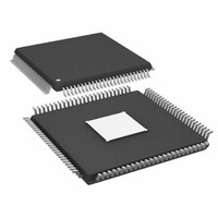
AD9957BSVZ Analog Devices Inc, AD9957BSVZ Datasheet - Page 39
AD9957BSVZ
Manufacturer Part Number
AD9957BSVZ
Description
IC DDS 1GSPS 14BIT IQ 100TQFP
Manufacturer
Analog Devices Inc
Datasheet
1.AD9957BSVZ-REEL.pdf
(64 pages)
Specifications of AD9957BSVZ
Resolution (bits)
14 b
Master Fclk
1GHz
Tuning Word Width (bits)
32 b
Voltage - Supply
1.8V, 3.3V
Operating Temperature
-40°C ~ 85°C
Mounting Type
Surface Mount
Package / Case
100-TQFP Exposed Pad, 100-eTQFP, 100-HTQFP, 100-VQFP
Frequency Range
60MHz To 1GHz
Rf Type
Quadrature
Supply Voltage Range
1.71V To 1.89V, 3.135V To 3.465
Rf Ic Case Style
TQFP
No. Of Pins
100
Operating Temperature Range
-40°C To +85°C
Operating Temperature (max)
85C
Operating Temperature (min)
-40C
Pin Count
100
Mounting
Surface Mount
Case Height
1mm
Screening Level
Industrial
Lead Free Status / RoHS Status
Lead free / RoHS Compliant
For Use With
AD9957/PCBZ - BOARD EVAL AD9957 QUADRATURE MOD
Lead Free Status / Rohs Status
Compliant
Available stocks
Company
Part Number
Manufacturer
Quantity
Price
Company:

Part Number:
AD9957BSVZ
Manufacturer:
AD
Quantity:
1 200
Company:
Part Number:
AD9957BSVZ
Manufacturer:
Analog Devices Inc
Quantity:
10 000
Part Number:
AD9957BSVZ
Manufacturer:
ADI/亚德诺
Quantity:
20 000
Company:
Part Number:
AD9957BSVZ-REEL
Manufacturer:
Analog Devices Inc
Quantity:
10 000
Part Number:
AD9957BSVZ-REEL
Manufacturer:
ADI/亚德诺
Quantity:
20 000


POWER-DOWN CONTROL
The AD9957 offers the ability to independently power down four
specific sections of the device. Power-down functionality applies
to the digital core, DAC, auxiliary DAC, and REFCLK input.
A power-down of the digital core disables the ability to update
the serial I/O port. However, the digital power-down bit can
still be cleared via the serial port to prevent the possibility of a
nonrecoverable state.
Software power-down is controlled through four independent
power-down bits in CFR1. Software control requires forcing the
EXT_PWR_DWN pin to a Logic 0 state. In this case, setting the
desired power-down bits (via the serial I/O port) powers down
the associated functional block; clearing the bits restores the
function.
Alternatively, all four functions can be simultaneously powered
down via external hardware control through the EXT_PWR_DWN
pin. Forcing this pin to Logic 1 powers down all four circuit
blocks, regardless of the state of the power-down bits. That is,
the independent power-down bits in CFR1 are ignored and
overridden when EXT_PWR_DWN is Logic 1.
Based on the state of the external power-down control bit, the
EXT_PWR_DWN pin produces either a full power-down or a
fast recovery power-down. The fast recovery power-down mode
maintains power to the DAC bias circuitry and the PLL, VCO,
and input section of the REFCLK circuitry. Although the fast
recovery power-down does not conserve as much power as the
full power-down, it allows the device to very quickly awaken
from the power-down state.
GENERAL-PURPOSE I/O (GPIO) PORT
The GPIO function is only available when the AD9957 is pro-
grammed for QDUC mode and the Blackfin interface mode is
active. Because the Blackfin serial interface uses only two of
the 18 parallel data port pins (D<5:4>), the remaining 16 pins
(D<17:6> and D<3:0>) are available as a GPIO port.
Rev. B | Page 39 of 64
Each of these 16 pins is assigned a unique bit in both the 16-bit
GPIO configuration register and the 16-bit GPIO data register.
The status of each bit in the GPIO configuration register assigns
the associated pin as either a GPIO input or output (0 = input,
1 = output) based on the data listed in Table 11.
When a GPIO pin is programmed as an output, the logic state
written to the associated bit of the GPIO data register (via the
serial I/O port) appears at the GPIO pin. When a GPIO pin is
programmed as an input, the logic state of the GPIO pin can be
read (via the serial I/O port) in the associated bit position in the
GPIO data register. Note that the GPIO data register does not
require an I/O update.
Table 11. GPIO Pins vs. Configuration and Data Register Bits
Pin Label
D17
D16
D15
D14
D13
D12
D11
D10
D9
D8
D7
D6
D3
D2
D1
D0
Configuration Bit
15
14
13
12
11
10
9
8
7
6
5
4
3
2
1
0
Data Bit
15
14
13
12
11
10
9
8
7
6
5
4
3
2
1
0
AD9957
Related parts for AD9957BSVZ
Image
Part Number
Description
Manufacturer
Datasheet
Request
R

Part Number:
Description:
D/A Converter Evaluation Board
Manufacturer:
Analog Devices Inc
Datasheet:


Part Number:
Description:
±1.7g Dual-Axis IMEMS Accelerometer Evaluation Board
Manufacturer:
Analog Devices Inc
Datasheet:

Part Number:
Description:
Inertial Sensor Evaluation System
Manufacturer:
Analog Devices Inc
Datasheet:
Part Number:
Description:
Manufacturer:
Analog Devices Inc
Datasheet:
Part Number:
Description:
Manufacturer:
Analog Devices Inc
Datasheet:
Part Number:
Description:
Manufacturer:
Analog Devices Inc
Datasheet:
Part Number:
Description:
Manufacturer:
Analog Devices Inc
Datasheet:
Part Number:
Description:
Manufacturer:
Analog Devices Inc
Datasheet:
Part Number:
Description:
Manufacturer:
Analog Devices Inc
Datasheet:
Part Number:
Description:
Manufacturer:
Analog Devices Inc
Datasheet:
Part Number:
Description:
Manufacturer:
Analog Devices Inc
Datasheet:
Part Number:
Description:
Manufacturer:
Analog Devices Inc
Datasheet: