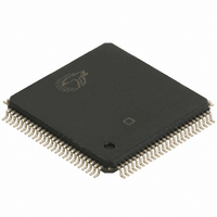
CY7C9689A-AXC Cypress Semiconductor Corp, CY7C9689A-AXC Datasheet - Page 21

CY7C9689A-AXC
Manufacturer Part Number
CY7C9689A-AXC
Description
IC TXRX HOTLINK 100LQFP
Manufacturer
Cypress Semiconductor Corp
Series
CY7Cr
Type
Transceiverr
Datasheet
1.CY7C9689A-AXC.pdf
(51 pages)
Specifications of CY7C9689A-AXC
Package / Case
100-LQFP
Voltage - Supply
4.5 V ~ 5.5 V
Mounting Type
Surface Mount
Product
PHY
Interface Type
Parallel
Supply Voltage (max)
6.5 V
Supply Voltage (min)
2 V
Supply Current
250 mA
Maximum Operating Temperature
+ 70 C
Minimum Operating Temperature
0 C
Mounting Style
SMD/SMT
Number Of Channels
2
Ic Interface Type
Parallel, Serial
Supply Voltage Range
4.5V To 5.5V
Operating Temperature Range
0°C To +70°C
Digital Ic Case Style
TQFP
No. Of Pins
100
Msl
MSL 3 - 168 Hours
No. Of Receivers
2
Rohs Compliant
Yes
Frequency Max
50MHz
Lead Free Status / RoHS Status
Lead free / RoHS Compliant
Number Of Drivers/receivers
-
Protocol
-
Lead Free Status / Rohs Status
Lead free / RoHS Compliant
Available stocks
Company
Part Number
Manufacturer
Quantity
Price
Company:
Part Number:
CY7C9689A-AXC
Manufacturer:
ALTERA
Quantity:
112
Company:
Part Number:
CY7C9689A-AXC
Manufacturer:
CY
Quantity:
86
Company:
Part Number:
CY7C9689A-AXC
Manufacturer:
CYPRESS
Quantity:
273
Company:
Part Number:
CY7C9689A-AXC
Manufacturer:
Cypress Semiconductor Corp
Quantity:
10 000
Part Number:
CY7C9689A-AXC
Manufacturer:
CYPRESS/赛普拉斯
Quantity:
20 000
Document #: 38-02020 Rev. *E
RXDATA bus output drivers are enabled when the device is
selected by RXEN being asserted in the RXCLK cycle immedi-
ately following that in which the device was addressed (CE is
sampled LOW), and RXEN being sampled by RXCLK. This
initiates a Receive FIFO read cycle.
Just as with the TXDATA bus on the Transmit Input Register,
the receive outputs are also mapped by the specific decoding
and bus-width selected by the ENCBYP, BYTE8/10 and
FIFOBYP inputs. These assignments are shown in
Table 6. Receiver Output Bus Signal Map
Notes
RXDATA Bus Output Bit
8. When BYTE8/10 is HIGH, received bit order is decoded form the serial stream and presented (MSB to LSB) at RXDATA[7,6,5,4] and RXDATA[3,2,1,0] or
9. When BYTE8/10 is LOW, received bit order is decoded form the serial stream and presented (MSB to LSB) at RXDATA[8,7,6,5,4] and RXDATA[9,3,2,1,0] or
10. First bit shifted into the receiver.
11. When ENCBYP is LOW and BYTE8/10 is HIGH, the received bit order is (LSB to MSB) RXD[0,1,2,3,4,5,6,7,8,9].
12. When ENCBYP is LOW and BYTE8/10 is LOW, the received bit order is (LSB to MSB) RXD[0,1,2,3,4,5,6,7,8,9,11,10].
RXDATA[8]/RXCMD[3]
RXDATA[9]/RXCMD[2]
RXCMD[3,2,1,0] as indicated by RXSC/D.
RXCMD[1,0] as indicated by RXSC/D.
RXDATA[0]
RXDATA[1]
RXDATA[2]
RXDATA[3]
RXDATA[4]
RXDATA[5]
RXDATA[6]
RXDATA[7]
RXCMD[1]
RXCMD[0]
RXSC/D
VLTN
Character Stream
Encoded 8-bit
RXDATA[0]
RXDATA[1]
RXDATA[2]
RXDATA[3]
RXDATA[4]
RXDATA[5]
RXDATA[6]
RXDATA[7]
RXCMD[3]
RXCMD[2]
RXCMD[1]
RXCMD[0]
RXSC/D
VLTN
[8]
Table
Pre-encoded 10-bit
Character Stream
6.
RXD[0]
RXD[1]
RXD[2]
RXD[3]
RXD[4]
RXD[5]
RXD[6]
RXD[7]
RXD[8]
RXD[9]
Receiver Decoder Mode
If the Receive FIFO and Decoder are bypassed, all received
characters are passed directly to the Receive Output Register.
If framing is enabled, and JK or LM sync characters have been
detected meeting the present framing requirements, the
output characters will appear on proper character boundaries.
If framing is disabled (RFEN is LOW) or sync characters have
not been detected in the data stream, the received characters
may not be output on their proper 10-bit boundaries. In this
mode, some form of external framing and decoding/descram-
bling must be used to recover the original source data.
[10, 11]
Character Stream
Encoded 10-bit
RXDATA[9]
RXDATA[0]
RXDATA[1]
RXDATA[2]
RXDATA[3]
RXDATA[4]
RXDATA[5]
RXDATA[6]
RXDATA[7]
RXDATA[8]
RXCMD[1]
RXCMD[0]
RXSC/D
VLTN
[1]
[9]
[9]
Pre-encoded 12-bit
Character Stream
CY7C9689A
RXD[0]
RXD[10]
RXD[11]
RXD[1]
RXD[2]
RXD[3]
RXD[4]
RXD[5]
RXD[6]
RXD[7]
RXD[8]
RXD[9]
Page 21 of 51
[10, 12]
[12]
[+] Feedback


