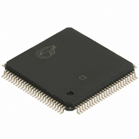
CY7C9689A-AXC Cypress Semiconductor Corp, CY7C9689A-AXC Datasheet - Page 33

CY7C9689A-AXC
Manufacturer Part Number
CY7C9689A-AXC
Description
IC TXRX HOTLINK 100LQFP
Manufacturer
Cypress Semiconductor Corp
Series
CY7Cr
Type
Transceiverr
Datasheet
1.CY7C9689A-AXC.pdf
(51 pages)
Specifications of CY7C9689A-AXC
Package / Case
100-LQFP
Voltage - Supply
4.5 V ~ 5.5 V
Mounting Type
Surface Mount
Product
PHY
Interface Type
Parallel
Supply Voltage (max)
6.5 V
Supply Voltage (min)
2 V
Supply Current
250 mA
Maximum Operating Temperature
+ 70 C
Minimum Operating Temperature
0 C
Mounting Style
SMD/SMT
Number Of Channels
2
Ic Interface Type
Parallel, Serial
Supply Voltage Range
4.5V To 5.5V
Operating Temperature Range
0°C To +70°C
Digital Ic Case Style
TQFP
No. Of Pins
100
Msl
MSL 3 - 168 Hours
No. Of Receivers
2
Rohs Compliant
Yes
Frequency Max
50MHz
Lead Free Status / RoHS Status
Lead free / RoHS Compliant
Number Of Drivers/receivers
-
Protocol
-
Lead Free Status / Rohs Status
Lead free / RoHS Compliant
Available stocks
Company
Part Number
Manufacturer
Quantity
Price
Company:
Part Number:
CY7C9689A-AXC
Manufacturer:
ALTERA
Quantity:
112
Company:
Part Number:
CY7C9689A-AXC
Manufacturer:
CY
Quantity:
86
Company:
Part Number:
CY7C9689A-AXC
Manufacturer:
CYPRESS
Quantity:
273
Company:
Part Number:
CY7C9689A-AXC
Manufacturer:
Cypress Semiconductor Corp
Quantity:
10 000
Part Number:
CY7C9689A-AXC
Manufacturer:
CYPRESS/赛普拉斯
Quantity:
20 000
Document #: 38-02020 Rev. *E
Table 7. HOTLink TAXI-compatible Encoder Patterns
Notes
39. Binary Input Data is the parallel input data which is input to the Transmitter and output from the Receiver. Binary bits are listed from left to right in the following
40. The ENCODED Symbols are shown here as “ones and zeros”, but are converted to and from an NRZI stream at the transmitter output and receiver input. NRZI
41. Encoded Serial Symbol bits are shifted out with the most significant bit (Left-most) of the most significant nibble coming out first.
42. Binary CMD is the parallel input data which is input to the Transmitter and output from the Receiver. Binary bits are listed from left to right in the following order:
43. While these Commands are legal data and will not disrupt normal operation if used occasionally, they may cause data errors if grouped into recurrent fields.
CY7C9689A HOTLink Receiver Switching Waveforms
RXDATA[9:8/RXCMD[2:3]
Output Enable Timing
RXDATA[7:0]
RXCMD[1:0]
order: 8-Bit mode (BYTE8/10 is HIGH and TXSC/D or RXSC/D is LOW)—TXDATA/RXDATA[7], [6], [5], [4], and TXDATA/RXDATA[3], [2], [1], [0]; 10-Bit mode
(BYTE8/10 is LOW and TXSC/D or RXSC/D is LOW)—TXDATA/RXDATA[8], [7], [6], [5], [4], and TXDATA/RXDATA[9], [3], [2], [1], [0].
represents a “one” as a state transition (either LOW-to-HIGH or HIGH-to-LOW) and a “zero” as no transition within the bit interval.
8-Bit mode (BYTE8/10 is HIGH and TXSC/D or RXSC/D is HIGH)—TXCMD/RXCMD[3], [2], [1], [0]; 10-Bit mode (BYTE8/10 is LOW and TXSC/D or RXSC/D
is HIGH)—TXCMD/RXCMD[1], [0].
Normal PLL operation cannot be guaranteed if one or more of these commands is continuously repeated.
Data
HEX
RXFULL
RXRST
RXCLK
0
1
RXEN
REFCLK
CE
Static Alignment
INA
INB
t
±
±
RXCES
4-bit Binary
4B/5B Encoder
Data
0000
0001
[41]
t
B
/2− t
SAMPLE WINDOW
SA
t
REFL
5-bit Encoded
Symbol
t
B
01001
11110
/2− t
[42, 43]
SA
Note 39
t
t
RXRSS
RXENS
t
REFH
Data
HEX
00
01
Error-Free Window
(continued)
INA
INB
t
t
RXCEH
±
±
RXRSH
t
t
t
RXZA
REFCLK
RXENH
5-bit Binary
t
RXOE
Data
00000
00001
BIT CENTER
5B/6B Encoder
OLD DATA
[41]
NO OPERATION
t
EFW
t
Note 40
B
t
BIT CENTER
RXAZ
6-bit Encoded
Symbol
CY7C9689A
010001
110110
Page 33 of 51
[42, 43]
[+] Feedback


