USB1T11AMTCX Fairchild Semiconductor, USB1T11AMTCX Datasheet - Page 4
USB1T11AMTCX
Manufacturer Part Number
USB1T11AMTCX
Description
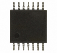
TRANSCEIVER UNIV BUS 14TSSOP
Manufacturer
Fairchild Semiconductor
Type
Transceiverr
Datasheet
1.USB1T11AMTC.pdf
(10 pages)
Specifications of USB1T11AMTCX
Number Of Drivers/receivers
1/1
Protocol
USB 1.1
Voltage - Supply
3.3V
Mounting Type
Surface Mount
Package / Case
14-TSSOP
Data Rate
12Mbps
Supply Current
5mA
Supply Voltage Range
3V To 3.6V
Driver Case Style
TSSOP
No. Of Pins
14
Operating Temperature Range
-40°C To +85°C
Interface
USB
Filter Terminals
SMD
Rohs Compliant
Yes
Data Rate Max
12Mbps
Lead Free Status / RoHS Status
Lead free / RoHS Compliant
Other names
USB1T11AMTCXTR
Available stocks
Company
Part Number
Manufacturer
Quantity
Price
Company:

Part Number:
USB1T11AMTCX
Manufacturer:
FSC
Quantity:
1 754
Part Number:
USB1T11AMTCX
Manufacturer:
FAIRCHILD/ن»™ç«¥
Quantity:
20 000


© 1999 Fairchild Semiconductor Corporation
USB1T11A • Rev. 1.0.4
Absolute Maximum Ratings
Stresses exceeding the absolute maximum ratings may damage the device. The device may not function or be
operable above the recommended operating conditions and stressing the parts to these levels is not recommended.
In addition, extended exposure to stresses above the recommended operating conditions may affect device
reliability. The absolute maximum ratings are stress ratings only.
Note:
1.
Recommended Operating Conditions
The Recommended Operating Conditions table defines the conditions for actual device operation. Recommended
operating conditions are specified to ensure optimal performance to the datasheet specifications. Fairchild does not
recommend exceeding them or designing to Absolute Maximum Ratings.
Symbol
I
Symbol
CC
T
V
V
The input and output negative voltage ratings may be exceeded if the input and output diode current ratings are
observed.
V
V
V
I
V
V
V
I
I
T
OK
/ I
STG
AI/O
CC
IK
I/O
O
CC
IN
O
IN
O
A
GND
DC Supply Voltage
DC Input Diode Current, V
Input Voltage
Input Voltage
Output Diode Current, V
Output Voltage
Output Source or Sink Current
(V
V
Storage Temperature Range
Power Supply Operating
Input Voltage
Input Range for AI/0
Output Voltage
Operating Ambient Temperature, Free Air
CC
O
= 0 to V
/ GND Current
CC
(1)
)
O
Parameter
Parameter
>V
IN
<0V
CC
or V
O
<0
V
D+/D- Pins
P
, V
M
4
, RCV Pins
Min.
Min.
3.0
-40
-60
0.5
0.5
0.5
0.5
0
0
0
V
V
CC
CC
Max.
Max.
+150
±100
±50
±15
±50
V
V
+85
-50
7.0
5.5
3.6
5.5
+ 0.5
+ 0.5
CC
CC
www.fairchildsemi.com
Unit
Unit
mA
mA
mA
mA
°C
°C
V
V
V
V
V
V
V
V
Related parts for USB1T11AMTCX
Image
Part Number
Description
Manufacturer
Datasheet
Request
R

Part Number:
Description:
Universal Serial Bus Transceiver
Manufacturer:
Fairchild Semiconductor
Datasheet:
Part Number:
Description:
Fairchild Semiconductor [IGBT MODULE]
Manufacturer:
Fairchild Semiconductor
Datasheet:

Part Number:
Description:
Discrete Semiconductor Modules
Manufacturer:
Fairchild Semiconductor
Part Number:
Description:
Discrete Semiconductor Modules
Manufacturer:
Fairchild Semiconductor
Part Number:
Description:
This N-Channel MOSFET is produced using Fairchild Semiconductor’s advanced Power Trench® process
Manufacturer:
Fairchild Semiconductor
Datasheet:
Part Number:
Description:
This N-Channel MOSFET is produced using Fairchild Semiconductor’s advanced Power Trench® process
Manufacturer:
Fairchild Semiconductor
Datasheet:
Part Number:
Description:
This N-Channel MOSFET is produced using Fairchild Semiconductor’s advanced PowerTrench® process
Manufacturer:
Fairchild Semiconductor
Datasheet:
Part Number:
Description:
This N-Channel MOSFET is produced using Fairchild Semiconductor’s advanced PowerTrench® process
Manufacturer:
Fairchild Semiconductor
Datasheet:
Part Number:
Description:
This N-Channel MOSFET is produced using Fairchild Semiconductor’s advanced Power Trench® process
Manufacturer:
Fairchild Semiconductor
Datasheet:
Part Number:
Description:
This N-Channel logic Level MOSFETs are produced using Fairchild Semiconductor‘s advanced Power Trench® process that has been special tailored to minimize the on-state resistance and yet maintain superior switching performance
Manufacturer:
Fairchild Semiconductor
Datasheet:
Part Number:
Description:
This N-Channel MOSFET is produced using Fairchild Semiconductor’s advanced Power Trench® process
Manufacturer:
Fairchild Semiconductor
Datasheet:
Part Number:
Description:
This N-Channel SyncFET™ is produced using Fairchild Semiconductor’s advanced PowerTrench® process
Manufacturer:
Fairchild Semiconductor
Datasheet:
Part Number:
Description:
This N-Channel SyncFET™ is produced using Fairchild Semiconductor’s advanced PowerTrench® process
Manufacturer:
Fairchild Semiconductor
Datasheet:
Part Number:
Description:
This N-Channel SyncFET™ is produced using Fairchild Semiconductor’s advanced PowerTrench® process
Manufacturer:
Fairchild Semiconductor
Datasheet:
Part Number:
Description:
This N-Channel logic Level MOSFETs are produced using Fairchild Semiconductor‘s advanced Power Trench® process that has been special tailored to minimize the on-state resistance and yet maintain superior switching performance
Manufacturer:
Fairchild Semiconductor
Datasheet: