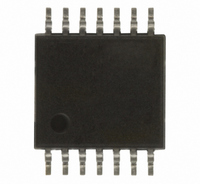
USB1T11AMTCX Fairchild Semiconductor, USB1T11AMTCX Datasheet - Page 6

USB1T11AMTCX
Manufacturer Part Number
USB1T11AMTCX
Description
TRANSCEIVER UNIV BUS 14TSSOP
Manufacturer
Fairchild Semiconductor
Type
Transceiverr
Datasheet
1.USB1T11AMTC.pdf
(10 pages)
Specifications of USB1T11AMTCX
Number Of Drivers/receivers
1/1
Protocol
USB 1.1
Voltage - Supply
3.3V
Mounting Type
Surface Mount
Package / Case
14-TSSOP
Data Rate
12Mbps
Supply Current
5mA
Supply Voltage Range
3V To 3.6V
Driver Case Style
TSSOP
No. Of Pins
14
Operating Temperature Range
-40°C To +85°C
Interface
USB
Filter Terminals
SMD
Rohs Compliant
Yes
Data Rate Max
12Mbps
Lead Free Status / RoHS Status
Lead free / RoHS Compliant
Other names
USB1T11AMTCXTR
Available stocks
Company
Part Number
Manufacturer
Quantity
Price
Company:
Part Number:
USB1T11AMTCX
Manufacturer:
FSC
Quantity:
1 754
Part Number:
USB1T11AMTCX
Manufacturer:
FAIRCHILD/ن»™ç«¥
Quantity:
20 000
© 1999 Fairchild Semiconductor Corporation
USB1T11A • Rev. 1.0.4
AC Electrical Characteristics D+/D- Pins, Full Speed
Over recommended range of supply voltage and operating free air temperature unless otherwise noted.
V
Driver Characteristics
Driver Timings
Receiver Timings
AC Electrical Characteristics D+/D- Pins, Low Speed
Over recommended range of supply voltage and operating free air temperature unless otherwise noted.
V
Driver Characteristics
Driver Timings
Receiver Timings
CC
CC
Symbol
Symbol
t
t
t
t
t
t
t
t
PLH
PLH
PLH
PLH
PHZ,
PZH,
PHZ,
PZH,
t
LR
V
V
= 3.0V to 3.6V, C
= 3.0V to 3.6V, C
t
t
t
t
t
t
R,
RFM
RFM
PLH
PLH
PHL
CRS
CRS
, t
, t
, t
, t
, t
t
t
t
t
t
F
PLZ
PZL
PHL
PHL
PLZ
PZL
PHL
PHL
LF
Rise and Fall Time
Rise/Fall Time Matching
Output Signal Crossover Voltage
Driver Propagation Delay
(V
Driver Disable Delay (/OE to D+/D-)
Driver Enable Delay (/OE to D+/D-)
Receiver Propagation Delay
D+/D- to RVC
Single-ended Receiver Delay
(D+/D- to V
Rise and Fall Time
Rise/Fall Time Matching
Output Signal Crossover Voltage
Driver Propagation Delay
(V
Driver Disable Delay (/OE to D+/D-)
Driver Enable Delay (/OE to D+/D-)
Receiver Propagation Delay
(D+/D- to RVC)
Single-ended Receiver Delay
(D+/D- to V
PO
PO
,V
,V
MO
MO
L
L
= 50Pf; R
= 200pF to 600pF; R
/F
/F
SEO
SEO
P
P
, V
, V
Parameter
Parameter
to D+/D-)
to D+/D-)
M
M
)
)
L
= kΩ on D+ to V
L
= 1.5kΩ on D- to V
CC
.
10 and 90%, Figure 4
t
Figure 4
Figure 6
Figure 6
Figure 5
Figure 5
Figure 5
10 and 90%, Figure 4
t
Figure 4
Figure 6
Figure 6
Figure 5
Figure 5
R
R
/ t
/ t
6
F
F
Conditions
Conditions
CC
.
Min.
Min.
1.3
1.3
90
75
80
4
T
T
A
A
=-40 to +85°C
=-40 to +85°C
Typ.
Typ.
Max.
Max.
110
300
120
300
205
2.0
2.0
20
18
13
17
16
19
13
18
28
8
www.fairchildsemi.com
Units
Units
ns
ns
ns
ns
ns
ns
ns
ns
ns
ns
ns
ns
ns
%
%
V
V


