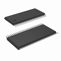
DS90CR286MTD/NOPB National Semiconductor, DS90CR286MTD/NOPB Datasheet

DS90CR286MTD/NOPB
Specifications of DS90CR286MTD/NOPB
*DS90CR286MTD/NOPB
DS90CR286MTD
Available stocks
Related parts for DS90CR286MTD/NOPB
DS90CR286MTD/NOPB Summary of contents
Page 1
... Block Diagrams DS90CR285 Order Number DS90CR285MTD See NS Package Number MTD56 TRI-STATE ® registered trademark of National Semiconductor Corporation. © 2004 National Semiconductor Corporation The 28 LVCMOS/LVTTL inputs can support a variety of signal combinations. For example, seven 4-bit nibbles or three 9-bit (byte + parity) and 1 control. Features n Single +3 ...
Page 2
Pin Diagrams for TSSOP Packages DS90CR285 Typical Application www.national.com 01291021 2 DS90CR286 01291022 01291023 ...
Page 3
... Absolute Maximum Ratings If Military/Aerospace specified devices are required, please contact the National Semiconductor Sales Office/ Distributors for availability and specifications. Supply Voltage ( CMOS/TTL Input Voltage −0. CMOS/TTL Output Voltage −0. LVDS Receiver Input Voltage −0. LVDS Driver Output Voltage −0. LVDS Output Short Circuit ...
Page 4
Electrical Characteristics Over recommended operating supply and temperature ranges unless otherwise specified Symbol Parameter TRANSMITTER SUPPLY CURRENT I Transmitter Supply Current Worst CCTW Case (with Loads) I Transmitter Supply Current Power CCTZ Down RECEIVER SUPPLY CURRENT I Receiver Supply Current ...
Page 5
Transmitter Switching Characteristics Over recommended operating supply and −40˚C to +85˚C ranges unless otherwise specified Symbol Parameter TPPos3 Transmitter Output Pulse Position for Bit3 TPPos4 Transmitter Output Pulse Position for Bit4 TPPos5 Transmitter Output Pulse Position for Bit5 TPPos6 Transmitter ...
Page 6
Receiver Switching Characteristics Over recommended operating supply and −40˚C to +85˚C ranges unless otherwise specified Symbol RSRC RxOUT Setup to RxCLK OUT (Figure 7) RHRC RxOUT Hold to RxCLK OUT (Figure 7) RCCD RxCLK IN to RxCLK OUT Delay (Figure ...
Page 7
AC Timing Diagrams (Continued) FIGURE 3. DS90CR286 (Receiver) CMOS/TTL Output Load and Transition Times FIGURE 4. DS90CR285 (Transmitter) Input Clock Transition Time Note 8: Measurements DIFF Note 9: TCCS measured between earliest and latest LVDS edges. ...
Page 8
AC Timing Diagrams FIGURE 6. DS90CR285 (Transmitter) Setup/Hold and High/Low Times FIGURE 7. DS90CR286 (Receiver) Setup/Hold and High/Low Times FIGURE 8. DS90CR285 (Transmitter) Clock In to Clock Out Delay FIGURE 9. DS90CR286 (Receiver) Clock In to Clock Out Delay www.national.com ...
Page 9
AC Timing Diagrams (Continued) FIGURE 10. DS90CR285 (Transmitter) Phase Lock Loop Set Time FIGURE 11. DS90CR286 (Receiver) Phase Lock Loop Set Time FIGURE 12. Seven Bits of LVDS in Once Clock Cycle 01291014 01291015 9 01291013 www.national.com ...
Page 10
AC Timing Diagrams FIGURE 13. 28 ParalIeI TTL Data Inputs Mapped to LVDS Outputs www.national.com (Continued) FIGURE 14. Transmitter Powerdown DeIay FIGURE 15. Receiver Powerdown Delay 10 01291016 01291017 01291018 ...
Page 11
AC Timing Diagrams (Continued) FIGURE 16. Transmitter LVDS Output Pulse Position Measurement 11 01291019 www.national.com ...
Page 12
AC Timing Diagrams www.national.com (Continued) FIGURE 17. Receiver LVDS Input Strobe Position 12 01291028 ...
Page 13
AC Timing Diagrams C — Setup and Hold Time (Internal data sampling window) defined by Rspos (receiver input strobe position) min and max Tppos — Transmitter output pulse position (min and max) RSKM ≥ Cable Skew (type, length) + Source ...
Page 14
DS90CR286 MTD56 (TSSOP) Package Pin Description — Channel Link Receiver (Continued) Pin Name I/O No. PLL GND I 2 Ground pin for PLL. LVDS Power supply pin for LVDS inputs. CC LVDS GND I 3 Ground pins ...
Page 15
Applications Information number of bypass capacitors, the PLL V FIGURE 20. CHANNEL LINK Decoupling Configuration CLOCK JITTER: The CHANNEL LINK devices employ a PLL to generate and recover the clock transmitted across the LVDS interface. The width of each bit ...
Page 16
Applications Information FIGURE 21. Single-Ended and Differential Waveforms www.national.com (Continued) 16 01291026 ...
Page 17
... BANNED SUBSTANCE COMPLIANCE National Semiconductor certifies that the products and packing materials meet the provisions of the Customer Products Stewardship Specification (CSP-9-111C2) and the Banned Substances and Materials of Interest Specification (CSP-9-111S2) and contain no ‘‘Banned Substances’’ as defined in CSP-9-111S2. ...


