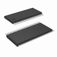
DS90CR286MTD/NOPB National Semiconductor, DS90CR286MTD/NOPB Datasheet - Page 5

DS90CR286MTD/NOPB
Manufacturer Part Number
DS90CR286MTD/NOPB
Description
IC RCVR 28BIT CHAN LINK 56TSSOP
Manufacturer
National Semiconductor
Type
Receiverr
Datasheet
1.DS90CR285MTDNOPB.pdf
(17 pages)
Specifications of DS90CR286MTD/NOPB
Number Of Drivers/receivers
0/4
Protocol
RS644
Voltage - Supply
3 V ~ 3.6 V
Mounting Type
Surface Mount
Package / Case
56-TSSOP
Supply Current
105mA
Supply Voltage Range
3V To 3.6V
Driver Case Style
TSSOP
No. Of Pins
56
Operating Temperature Range
-40°C To +85°C
Msl
MSL 2 - 1 Year
Device Type
Clock
Filter Terminals
SMD
Rohs Compliant
Yes
Esd Hbm
7kV
Lead Free Status / RoHS Status
Lead free / RoHS Compliant
Other names
*DS90CR286MTD
*DS90CR286MTD/NOPB
DS90CR286MTD
*DS90CR286MTD/NOPB
DS90CR286MTD
Available stocks
Company
Part Number
Manufacturer
Quantity
Price
Company:
Part Number:
DS90CR286MTD/NOPB
Manufacturer:
NS
Quantity:
339
TPPos3
TPPos4
TPPos5
TPPos6
TPPos0
TPPos1
TPPos2
TPPos3
TPPos4
TPPos5
TPPos6
TCIP
TCIH
TCIL
TSTC
THTC
TCCD
TPLLS
TPDD
CLHT
CHLT
RSPos0
RSPos1
RSPos2
RSPos3
RSPos4
RSPos5
RSPos6
RSPos0
RSPos1
RSPos2
RSPos3
RSPos4
RSPos5
RSPos6
RSKM
RCOP
RCOH
RCOL
Transmitter Switching Characteristics
Symbol
Symbol
Over recommended operating supply and −40˚C to +85˚C ranges unless otherwise specified
Receiver Switching Characteristics
Over recommended operating supply and −40˚C to +85˚C ranges unless otherwise specified
Transmitter Output Pulse Position for Bit3
Transmitter Output Pulse Position for Bit4
Transmitter Output Pulse Position for Bit5
Transmitter Output Pulse Position for Bit6
Transmitter Output Pulse Position for Bit0
(Note 6) (Figure 16)
Transmitter Output Pulse Position for Bit1
Transmitter Output Pulse Position for Bit2
Transmitter Output Pulse Position for Bit3
Transmitter Output Pulse Position for Bit4
Transmitter Output Pulse Position for Bit5
Transmitter Output Pulse Position for Bit6
TxCLK IN Period (Figure 6 )
TxCLK IN High Time (Figure 6)
TxCLK IN Low Time (Figure 6)
TxIN Setup to TxCLK IN (Figure 6)
TxIN Hold to TxCLK IN (Figure 6)
TxCLK IN to TxCLK OUT Delay
8)
Transmitter Phase Lock Loop Set (Figure 10)
Transmitter Powerdown Delay (Figure 14)
CMOS/TTL Low-to-High Transition Time (Figure 3)
CMOS/TTL High-to-Low Transition Time (Figure 3)
Receiver Input Strobe Position for Bit 0 (Note 7)(Figure 17)
Receiver Input Strobe Position for Bit 1
Receiver Input Strobe Position for Bit 2
Receiver Input Strobe Position for Bit 3
Receiver Input Strobe Position for Bit 4
Receiver Input Strobe Position for Bit 5
Receiver Input Strobe Position for Bit 6
Receiver Input Strobe Position for Bit 0 (Note 6)(Figure 17)
Receiver Input Strobe Position for Bit 1
Receiver Input Strobe Position for Bit 2
Receiver Input Strobe Position for Bit 3
Receiver Input Strobe Position for Bit 4
Receiver Input Strobe Position for Bit 5
Receiver Input Strobe Position for Bit 6
RxIN Skew Margin (Note 5) (Figure 18)
RxCLK OUT Period (Figure 7)
RxCLK OUT High Time (Figure 7)
RxCLK OUT Low Time (Figure 7)
Parameter
@
Parameter
25˚C,V
CC
f = 66 MHz
=3.3V (Figure
5
(Continued)
f = 40 MHz
f = 66 MHz
f = 40 MHz
f = 66 MHz
f = 40 MHz
f = 66 MHz
f = 40 MHz
f = 66 MHz
0.35T
0.35T
10.2
13.7
17.3
21.0
−0.4
10.6
12.8
Min
1.8
4.0
6.2
8.4
2.5
15
0
3
10.4
13.9
17.6
21.2
11.0
13.2
0.5T
0.5T
Typ
2.2
4.4
6.6
8.8
3.7
11.6
15.1
18.8
22.5
11.7
13.9
10.0
Min
490
400
1.0
4.5
8.1
0.7
2.9
5.1
7.3
9.5
6.0
4.0
6.0
0
T
15
11.9
15.6
19.2
22.9
12.1
14.3
10.0
13.0
Typ
2.2
2.2
1.4
5.0
8.5
1.1
3.3
5.5
7.7
9.9
6.1
7.8
T
0.65T
0.65T
Max
11.0
14.6
18.2
21.8
11.3
13.5
100
0.3
2.5
4.7
6.9
9.1
5.5
50
10
Max
2.15
9.15
12.6
16.3
19.9
23.6
10.2
12.4
14.6
5.0
5.0
5.8
1.4
3.6
5.8
8.0
50
www.national.com
Units
Units
ms
ns
ns
ns
ns
ns
ns
ns
ns
ns
ns
ns
ns
ns
ns
ns
ns
ns
ns
ns
ns
ns
ns
ns
ns
ns
ns
ns
ns
ns
ns
ns
ns
ns
ns
ps
ps
ns
ns
ns
ns
ns


