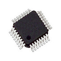
MC100EP445FA ON Semiconductor, MC100EP445FA Datasheet - Page 13

MC100EP445FA
Manufacturer Part Number
MC100EP445FA
Description
Manufacturer
ON Semiconductor
Datasheet
1.MC100EP445FA.pdf
(19 pages)
Specifications of MC100EP445FA
Operating Temperature (max)
85C
Operating Temperature (min)
-40C
Package Type
LQFP
Pin Count
32
Mounting
Surface Mount
Lead Free Status / Rohs Status
Not Compliant
Available stocks
Company
Part Number
Manufacturer
Quantity
Price
Company:
Part Number:
MC100EP445FAG
Manufacturer:
ON Semiconductor
Quantity:
120
Company:
Part Number:
MC100EP445FAG
Manufacturer:
ON Semiconductor
Quantity:
10 000
Company:
Part Number:
MC100EP445FAR2
Manufacturer:
ON Semiconductor
Quantity:
10 000
Company:
Part Number:
MC100EP445FAR2G
Manufacturer:
ON Semiconductor
Quantity:
10 000
correctly, the start bit for conversion can be moved using the
SYNC input pin (pin 2). Asynchronously asserting the
SYNC pin will force the internal clock to swallow a clock
pulse, effectively shifting a bit from the Q
as shown in Figure 10 and Figure 11. For CKSEL LOW, a
single pulse applied asynchronously for two consecutive
CKSEL
SYNC
PCLK
To allow the user to synchronize the output byte data
SINA
CLK
Q0
Q1
Q2
Q3
Q4
Q5
Q6
Q7
Figure 10. Timing Diagram A. 1:8 Serial to Parallel Conversion with SYNC Pulse at CKSEL LOW
D0
D1 D2 D3
2 Clock Cycles for SYNC
D4 D5 D6
1
2
D7 D8
Á
n
À
to the Q
D9 D10 D11 D12 D13 D14 D15 D16 D17 D18 D19 D20 D21 D22 D23 D24
Next Triggering Edge of Clock
Bit D8 is Swallowed
n−1
http://onsemi.com
output
13
D0
D1
D2
D3
D4
D5
D6
D7
clock cycles shifts the start bit for conversion from Q
Q
pulse width of SYNCÀ on the next triggering edge of
clockÁ (either on the rising or the falling edge of the clock).
Each additional shift requires an additional pulse to be
applied to the SYNC pin. (See Figure 10)
n−1
. The bit is swallowed following the two clock cycle
D10
D12
D13
D14
D15
D16
D11
D9
D17
D18
D19
D20
D21
D22
D23
D24
n
to


