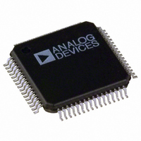
ADV7305AKST Analog Devices Inc, ADV7305AKST Datasheet - Page 51

ADV7305AKST
Manufacturer Part Number
ADV7305AKST
Description
IC ENCODER VIDEO 14BIT 64LQFP
Manufacturer
Analog Devices Inc
Type
Video Encoderr
Datasheet
1.ADV7305AKST.pdf
(68 pages)
Specifications of ADV7305AKST
Applications
DVD, SD/HD
Voltage - Supply, Analog
2.5V
Voltage - Supply, Digital
2.5V
Mounting Type
Surface Mount
Package / Case
64-LQFP
Number Of Dac's
6
Adc/dac Resolution
14b
Screening Level
Commercial
Package Type
LQFP
Pin Count
64
Lead Free Status / RoHS Status
Lead free / RoHS Compliant
Available stocks
Company
Part Number
Manufacturer
Quantity
Price
Company:
Part Number:
ADV7305AKST
Manufacturer:
SAMSUNG
Quantity:
200
To avoid crosstalk between the DAC outputs, it is recommended
to leave as much space as possible between the tracks of the
individual DAC output pins.
Supply Decoupling
Noise on the analog power plane can be further reduced by the
use of decoupling capacitors. Optimum performance is achieved
by the use of 0.1 µF ceramic capacitors. Each of the group of
V
ground. This should be done by placing the capacitors as close
as possible to the device with the capacitor leads as short as
possible, thus minimizing lead inductance.
Digital Signal Interconnect
The digital signal lines should be isolated as much as possible
from the analog outputs and other analog circuitry. Digital
signal lines should not overlay the analog power plane. Due to
REV. A
AA
, V
DD
, or V
DD_IO
pins should be individually decoupled to
UNUSED INPUTS SHOULD BE GROUNDED
V
V
AA
AA
47k
4.7 F
6.3V
680R
820pF
3.9nF
0.1 F
COMP1
GND_IO AGND DGND
S0–S9
V
C0–C9
Y0–Y9
RESET
CLKIN_B
CLKIN_A
EXT_LF
S_HSYNC
S_VSYNC
S BLANK
P_HSYNC
P_VSYNC
P_BLANK
AA
0.1 F
Figure 79. Circuit Layout
COMP2
ADV7304A/
ADV7305A
V
AA
POWER SUPPLY DECOUPLING FOR
V
AA
EACH POWER SUPPLY GROUP
V
11, 57
DD
–51–
DAC A
DAC B
DAC C
DAC D
DAC E
DAC F
10, 56
ALSB
SCLK
R
R
V
V
SDA
SET1
SET2
REF
DD_IO
I
2
C
the high clock rates used, long clock lines to the ADV7304A/
ADV7305A should be avoided to minimize noise pickup. Any
active pull-up termination resistors for the digital inputs should
be connected to the digital power plane and not the analog
power plane.
Analog Signal Interconnect
The ADV7304A/ADV7305A should be located as close as pos-
sible to the output connectors, thus minimizing noise pickup
and reflections due to impedance mismatch. For optimum per-
formance, the analog outputs should each be source and load
terminated, as shown in Figure 79. The termination resistors
should be as close as possible to the ADV7304A/ADV7305A to
minimize reflections.
Any unused inputs should be tied to ground.
10nF
1520
10nF
150
150
150
150
150
150
10nF
1520
0.1 F
0.1 F
SD CVBS/GREEN/Y
SD LUMA/BLUE/U
SD CHROMA/RED/V
HD Y/GREEN
HD Pb/BLUE
HD Pr/RED
0.1 F
V
DD_IO
V
V
V
AA
DD
DD_IO
5k
V
V
DD_IO
DD_IO
5k
5k
ADV7304A/ADV7305A
V
DD_IO
5k
I
BUS
2
C


