STA016AP STMicroelectronics, STA016AP Datasheet
STA016AP
Specifications of STA016AP
Available stocks


Related parts for STA016AP


STA016AP Summary of contents
Page 1
FEATURES SINGLE CHIP MPEG LAYER 3 DECODER SUPPORTING: – All features specified for Layer III in ISO/IEC 11172-3 (MPEG 1 Audio) – All features specified for Layer III in ISO/IEC 13818-3.2 (MPEG 2 Audio) – Lower sampling frequencies syntax ...
Page 2
STA016A 2 DESCRIPTION The STA016A is a single chip MPEG 1, 2 and 2.5 Layer III audio decoder with embedded CDROM decoding capability. It can be easily connected to most existing CDDSP devices via a software configurable serial link. A ...
Page 3
OVERVIEW The device can decode/process data coming from three possible sources, as showed in Figure 2: CDDSP serial link: using this input interface, besides MP3 encoded data CD, it's possible to playback also standard Audio CD using the available ...
Page 4
STA016A Figure 4. Layers performed by embedded DSP firmware The whole CDROM and file-system decoding task is performed by embedded firmware. The application MCU, basically, must manage CDDSP device according to STA016A requests. Three basic command flows exist: MCU -> ...
Page 5
Table 5. PIN DESCRIPTION PIN Pin Name 1 CD_LRCK 3 CD_SDI 2 CD_BCK 9 BS_SDI 7 BS_LRCK 8 BS_BCK 4 DREQ 13 BCKI 14 SDI 12 LRCKI 20 LRCKO 22 SDO 21 BCKO 19 OSCK 55 GPSO_CK 54 GPSO_SDO 56 ...
Page 6
STA016A Table 5. PIN DESCRIPTION (continued) PIN Pin Name 60 STB 59 RQST 63 SCL 64 SDA 17 XTI 18 XTO 25 CLKOUT 15 -RESET 16 -TESTEN 40 FILT0 38 FILT1 39 PLL_VCC 41 PLL_GND 5 VDD_1 10 VDD_2 29 ...
Page 7
ELECTRICAL CHARACTERISTCS (T = 25° unless otherwise specified) amb g Table 6. DC OPERATING CONDITIONS Symbol V Power Supply Voltage DD V Power Supply Voltage CC PLL_V Power Supply Voltage CC Table 7. GENERAL INTERFACE ELECTRICAL ...
Page 8
STA016A 5 HOST REGISTERS The following table gives a description of STA016A register list. The STA016A device includes 256 I scribed. The undocumented registers are reserved or unused. These registers must never be accessed (in Read or in Write mode). ...
Page 9
Table 11. REGISTER MAP BY FUNCTION Register function VERSION PLL_AUDIO_CONFIGURATION PLL_SYSTEM_CONFIGURATION I2Sout_CONFIGURATION GPSO_CONFIGURATION I2Sin_CONFIGURATION Hex Dec 0x00 0 VERSION 0x01 1 IDENT 0xD3 211 SOFT_VERSION 0xDC 220 PLL_AUDIO_PEL_192 0xDD 221 PLL_AUDIO_PEH_192 0xDE 222 PLL_AUDIO_NDIV_192 0xDF 223 PLL_AUDIO_XDIV_192 0xE0 224 PLL_AUDIO_MDIV_192 ...
Page 10
STA016A Register function CDBSA_CONFIGURATION BSB_CONFIGURATION CD_CONFIGURATION 10/43 Hex Dec 0x5A 90 INPUT_CONF 0x5B 91 I_AUDIO_CONFIG_1 0x5C 92 I_AUDIO_CONFIG_2 0x5D 93 I_AUDIO_CONFIG_3 0x5E 94 I_AUDIO_CONFIG_4 0x5F 95 I_AUDIO_CONFIG_5 0x60 96 I_AUDIO_CONFIG_6 0x61 97 I_AUDIO_CONFIG_7 0x62 98 I_AUDIO_CONFIG_8 0x63 99 I_AUDIO_CONFIG_9 0x64 ...
Page 11
Register function Hex 0x86 0x87 0x88 0x89 0x8A 0x8B 0x8C 0x8D 0x8E 0x8F 0x90 0x91 0x92 0x93 0x94 0x95 0x96 0x97 0x98 0x99 0x9A 0x9B 0x9C 0x9D 0x9E 0x9F 0xA0 0xA1 0xA2 0xA3 0xA4 0xA5 0xA6 Dec Name 134 CD_SONG_INFO_C1 ...
Page 12
STA016A Register function COMMAND 12/43 Hex Dec 0xA7 167 NB_OF_CUR_TRACK 0xA8 168 NB_OF_CUR_DIR 0xA9 169 CD_CUR_STATUS 0xAA 170 CD_TRACK_FORMAT 0xAB 171 CD_NB_OF_SUB_DIR 0xAC 172 CD_NB_OF_SUB_FILE 0xAD 173 DIRECTORY_LEVEL 0xAE 174 DIR_IDENTIFIER_B1 0xAF 175 DIR_IDENTIFIER_B2 0xB0 176 DIR_IDENTIFIER_B3 0xB1 177 DIR_IDENTIFIER_B4 ...
Page 13
Register function STATUS BYPASSA_CONFIGURATION MP3_CONFIGURATION RESERVED MIX_CONFIGURATION TONE_CONFIGURATION Hex Dec 0xCC 204 STATUS_MODE 0xCD 205 STATUS_CHAN_NB 0xCE 206 STATUS_SF 0x6F 111 STATUS_FE 0xD4 212 HEADER_1 0xD5 213 HEADER_2 0xD6 214 HEADER_3 0xD7 215 HEADER_4 0xD8 216 HEADER_5 0xD9 217 HEADER_6 ...
Page 14
STA016A 6 REGISTER DESCRIPTION 6.1 VERSION registers description 6.1.1 VERSION : Address : 0x00 (0) Type : RO - DWT Software Reset : 0x10 Hardware Reset : 0x10 Description : The VERSION register is Read-only ...
Page 15
Description : This register must contain a NDIV value that enables the audio PLL to generate a frequency of ofact*192 kHz for the PCMCK.See table 1, 2 & 3. Default value at soft reset assume : – ofact == 256 ...
Page 16
STA016A 6.2.9 PLL_AUDIO_XDIV_176 : Address : 0xE4 (228) Type : RW - DEC Software Reset : 2 Description : This register must contain a XDIV value that enables the audio PLL to generate a frequency ...
Page 17
Description : This register must contain a XDIV value that enables the system PLL to generate a frequency of 50 MHZ for the SYSCK. See table 4. Default value at soft reset assume : – external crystal provide a CRYCK ...
Page 18
STA016A Type : RW - DEC Software Reset : 10 Description : This register must contain a MDIV value that enables the system PLL to generate a frequency of 42.5 MHz for the SYSCK.See table 4. Default value at soft ...
Page 19
Table 13. . CR1 CR0 Comment 0 0 Left channel is mapped on the left output. Right channel is mapped on the right output Left channel is duplicated on both output channels. ...
Page 20
STA016A 6.6.2 I_AUDIO_CONFIG_1 CF7 CF6 CF5 CF4 CF3 Address : 0x5B (91) Type : RW - DEC Software Reset : 0 Description : If INPUT_CONF == 1, this register configure the I2Sin interface Table 16. ...
Page 21
CDBSA_CONFIGURATION registers description 6.7.1 INPUT_CONF : Address : 0x5A (90) Type : RW - DEC Software Reset : 0 Description : If set to 1 enable the configurability of the CD & BS input ...
Page 22
STA016A Table 20. . Bit Comment CF8 Relative synchro : 0 : synchro with first data bit 1 : synchro one bit before first data bit CF9 Data reception configuration : 0 : LSB first 1 : MSB first CF10 ...
Page 23
I_AUDIO_CONFIG_8 : MA31 MA30 MA29 MA28 MA27 MA26 MA25 MA24 Address : 0x62 (98) Type : RW - DEC Software Reset : 0 Description : If INPUT_CONF == 1, those registers are used to ...
Page 24
STA016A If set to 1 enable the configurability of the BSB input interfaces in burst mode thanks to following register, else disable this configurability and take embedded default configuration. Note that this embedded default configuration can be retrieved by user ...
Page 25
This specifies the number of track to play. 6.9.3 REQUIRED_DIR : Address : 0x43 (67) Type : RW - ABO Software Reset : 0 Description : This register specifies the number of directory to play. ...
Page 26
STA016A Description : This register specifies to the CD module the second location requested. 6.9.8 SECTOR_REQ : Address : 0x49 (73) Type : RO - AEC Software Reset : 0 Description : This register specifies ...
Page 27
CD_SONG_TYPE_INFO : Address : 0xA6 (166) Type : RO - AEC Software Reset : 0 Description : This register specifies the kind of current information contained in the Table 26. Value Signification 0 information ...
Page 28
STA016A 6.9.19 CD_TRACK_FORMAT : Address : 0xAA (170) Type : RO - AEC Software Reset : 0 Description : This register specifies the format of the played track considering the extension name. Only 1 bit ...
Page 29
EXTRACT_BYTE_IDX_Bn Address : 0xB6 (182) to 0xB8 (185) Type : RW - ABO Software Reset : 0 Description : th This register specifies the n byte of the index of the byte block to ...
Page 30
STA016A Description : This register select the decoding data flux according the mode written in following table Table 30. . Bit(7:0) 0 CD_MP3 1 CD_BYPASSA 2 RESERVED 3 BSB_MP3 4 RESERVED 5 RESERVED 6 RESERVED 7 BSA_BYPASSA 8 RESERVED 9 ...
Page 31
Description : For decoders having PAUSE abilities (see each de- coder configuration), if set to 0 disable the pause of the decoder, if set to 1 enable the pause of the de- coder. Note that during a PAUSE the input ...
Page 32
STA016A 6.11.5 HEADER _n Address : 0xD4 (212) to 0xD9 (217) Type : RO - EDF Software Reset : 0 Description : This register give the nth byte of the header of the frame currently ...
Page 33
MIX_CONFIGURATION registers description 6.13.1 MIX_MODE Address : 0x75 (117) Type : RW - ABO Software Reset : 2 Description : This register selectes the mode of mix/volume control Table 35. : Value 0 diseable ...
Page 34
STA016A Description : This register specifies the high cut frequency: fcut(in Hz)=(TONE_FCUTH+1)*50. 6.14.3 TONE_FCUTL : Address : 0x7C(124) Type : RW - ABO Software Reset : 10 Description : This register specifies the low cut ...
Page 35
Table 37. values to configure audio PLL for ofact==384 This table give values to configure the audio PLL according CRYCK so that to generate a PCMCK == 384*SF. Register PLL_AUDIO_PEL_192 PLL_AUDIO_PEH_192 PLL_AUDIO_NDIV_192 PLL_AUDIO_XDIV_192 PLL_AUDIO_MDIV_192 PLL_AUDIO_PEL_176 PLL_AUDIO_PEH_176 PLL_AUDIO_NDIV_176 PLL_AUDIO_XDIV_176 PLL_AUDIO_MDIV_176 Table ...
Page 36
STA016A Table 39. values to configure system PLL for SYSCK. This table give values to configure the system PLL according CRYCK so that to generate a SYSCK == 50MHz. or SYSCK == 42.5MHz. Register PLL_SYSTEM_PEL_50 PLL_SYSTEM_PEH_50 PLL_SYSTEM_NDIV_50 PLL_SYSTEM_XDIV_50 PLL_SYSTEM_MDIV_50 PLL_SYSTEM_PEL_42_5 ...
Page 37
NOTATIONS ABO : After BOot (see I). AEC : After External Config (see I). BCK : Bit ClocK BSA : BitStream input interface in Audio mode. BSB : BitStream input interface in Burst mode BitStream input interface. ...
Page 38
STA016A 7.3 TTL Schmitt Trigger Inpud Pad Buffer, 3V capable / Pin numbers:17, 60 7.4 TTL Inpud Pad Buffer, 3V capable with Pull-Up / Pin numbers:15 7.5 TTL Schmitt Trigger Bidir Pad Buffer, with Pull-up, 4mA, ...
Page 39
INTLINE[0] pin). 8.0.1 Reading a request from mmdsp : MMDSP write its request inside dedicated host registers (mainly H70 to H78 and H134 to H169), then it signals to cd_module that it must read a request by sending the ...
Page 40
STA016A Figure 8. Block diagram for answer to a sector request from dsp. Hxx: host register number xx 40/43 power on IT_REQ occured H70==18 read minute in H71 please check with rest of documentation read second in H72 read frame ...
Page 41
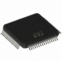
Figure 9. TQFP64 Mechanical Data & Package Dimensions mm DIM. MIN. TYP. MAX. A 1.60 A1 0.05 0.15 A2 1.35 1.40 1.45 B 0.17 0.22 0.27 C 0.09 D 11.80 12.00 12.20 D1 9.80 10.00 10.20 D3 7.50 e 0.50 ...
Page 42
STA016A Table 41. Revision History Date Revision July 2004 42/43 1 First Issue Description of Changes ...
Page 43
... No license is granted by implication or otherwise under any patent or patent rights of STMicroelectronics. Specifications mentioned in this publication are subject to change without notice. This publication supersedes and replaces all information previously supplied. STMicroelectronics products are not authorized for use as critical components in life support devices or systems without express written approval of STMicroelectronics ...