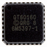
QT60160-ISG Atmel, QT60160-ISG Datasheet - Page 4

QT60160-ISG
Manufacturer Part Number
QT60160-ISG
Description
SENSOR IC MTRX TOUCH16KEY 32-QFN
Manufacturer
Atmel
Series
QMatrix™r
Type
Capacitiver
Datasheet
1.QT60160-ISG.pdf
(26 pages)
Specifications of QT60160-ISG
Number Of Inputs/keys
16 Key
Resolution (bits)
10 b
Data Interface
I²C, Serial, SPI™
Voltage Reference
External
Voltage - Supply
1.8V, 3.3V, 5V
Current - Supply
4.6mA
Operating Temperature
-40°C ~ 85°C
Mounting Type
Surface Mount
Package / Case
32-MLF®, QFN
Output Type
*
Interface
*
Input Type
*
Operating Supply Voltage
1.8 V to 5.5 V
Maximum Operating Temperature
+ 85 C
Mounting Style
SMD/SMT
Minimum Operating Temperature
- 40 C
Lead Free Status / RoHS Status
Lead free / RoHS Compliant
Other names
427-1125-2
Available stocks
Company
Part Number
Manufacturer
Quantity
Price
Company:
Part Number:
QT60160-ISG
Manufacturer:
NSC
Quantity:
622
Company:
Part Number:
QT60160-ISG QS129
Manufacturer:
LTC
Quantity:
1 190
The Cs should be connected as shown in Figure 2.7, page 9.
The value of these capacitors is not critical but 4.7nF is
recommended for most cases. They should be 10 percent
X7R ceramics. If the transverse capacitive coupling from X to
Y is large enough the voltage on a Cs capacitor can saturate,
destroying gain. In such cases the burst length should be
reduced and/or the Cs value increased. See Section 2.4.
If a Y line is not used its corresponding Cs capacitor may be
omitted and the pins left floating.
2.4 Sample Capacitor Saturation
Cs voltage saturation at a pin YnB is shown in Figure 2.1
Saturation begins to occur when the voltage at a YnB pin
becomes more negative than -0.25V at the end of the burst.
This nonlinearity is caused by excessive voltage
accumulation on Cs inducing conduction in the pin protection
diodes. This badly saturated signal destroys key gain and
introduces a strong thermal coefficient which can cause
'phantom' detection. The cause of this is either from the burst
length being too long, the Cs value being too small, or the
X-Y transfer coupling being too large. Solutions include
loosening up the key structure interleaving, more separation
of the X and Y lines on the PCB, increasing Cs, and
decreasing the burst length.
Increasing Cs will make the part slower; decreasing burst
length will make it less sensitive. A better PCB layout and a
looser key structure (up to a point) have no negative effects.
Cs voltages should be observed on an oscilloscope with the
matrix layer bonded to the panel material; if the Rs side of
any Cs ramps more negative than -0.25 volts during any burst
(not counting overshoot spikes which are probe artifacts),
there is a potential saturation problem.
Figure 2.2 shows a defective waveform similar to that of 2.1,
but in this case the distortion is caused by excessive stray
capacitance coupling from the Y line to AC ground ; for
example, from running too near and too far alongside a
ground trace, ground plane, or other traces. The excess
coupling causes the charge-transfer effect to dissipate a
significant portion of the received charge from a key into the
stray capacitance. This phenomenon is more subtle; it can be
best detected by increasing BL to a high count and watching
what the waveform does as it descends towards and below
-0.25V. The waveform will appear deceptively straight, but it
will slowly start to flatten even before the -0.25V level is
reached.
A correct waveform is shown in Figure 2.3. Note that the
bottom edge of the bottom trace is substantially straight
(ignoring the downward spikes).
Unlike other QT circuits, the Cs capacitor values on QT60xx 0
devices have no effect on conversion gain. However , they do
affect conversion time.
Unused Y lines should be left open.
2.5 Sample Resistors
There are three sample resistors (Rs) used to perform
single-slope ADC conversion of the acquired charge on each
Cs capacitor. These resistors directly control acquisition gain;
larger values of Rs will proportionately increase signal gain.
For most applications Rs should be 1M ✡. Unused Y lines do
not require an Rs resistor.
lQ
4
2.6 Signal Levels
Quantum’s QmBtn software makes it is easy to observe the
absolute level of signal received by the sensor on each key.
The signal values should normally be in the range of 200 to
750 counts with properly designed key shapes and values of
Rs. However, long adjacent runs of X and Y lines can also
artificially boost the signal values, and induce signal
saturation; this is to be avoided. The X-to-Y coupling should
come mostly from intra-key electrode coupling, not from stray
X-to-Y trace coupling.
Figure 2.2 VCs - Poor Gain, Nonlinear During Burst
X Drive
X Drive
(Burst too long, or Cs too small, or X-Y transcapacitance too large)
Figure 2.4 X-Drive Pulse Roll-off and Dwell Time
Dwell time
X Drive
Y gate
YnB
X drive
YnB
YnB
Figure 2.1 VCs - Nonlinear During Burst
The Dwell time is fixed at ~500ns - see Section 2.7
(Excess capacitance from Y line to Gnd)
Figure 2.3 VCs - Correct
Lost charge due to
inadequate settling
before end of dwell time
QT60240-ISG R8.06/0906


