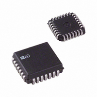
AD698APZ Analog Devices Inc, AD698APZ Datasheet - Page 5

AD698APZ
Manufacturer Part Number
AD698APZ
Description
IC LVDT SIGNAL COND 28-PLCC
Manufacturer
Analog Devices Inc
Type
Signal Conditionerr
Datasheet
1.AD698APZ.pdf
(12 pages)
Specifications of AD698APZ
Input Type
Voltage
Output Type
Voltage
Interface
LVDT
Current - Supply
15mA
Mounting Type
Surface Mount
Package / Case
28-LCC (J-Lead)
Bandwidth
20kHz
Supply Voltage Min
13V
Supply Voltage Max
36V
Digital Ic Case Style
LCC
No. Of Pins
28
Operating Temperature Range
-40°C To +85°C
Msl
MSL 5 - 48 Hours
Supply Voltage Range
13V To 36V
Audio Ic Case Style
PLCC
Base Number
698
Rohs Compliant
Yes
Lead Free Status / RoHS Status
Lead free / RoHS Compliant
Lead Free Status / RoHS Status
Lead free / RoHS Compliant, Lead free / RoHS Compliant
Available stocks
Company
Part Number
Manufacturer
Quantity
Price
Company:
Part Number:
AD698APZ
Manufacturer:
Analog Devices Inc
Quantity:
135
Part Number:
AD698APZ
Manufacturer:
ADI/亚德诺
Quantity:
20 000
REV. B
THEORY OF OPERATION
A block diagram of the AD698 along with an LVDT (linear
variable differential transformer) connected to its input is shown
in Figure 5 below. The LVDT is an electromechanical trans-
ducer—its input is the mechanical displacement of a core, and
its output is an ac voltage proportional to core position. Two
popular types of LVDTs are the half-bridge type and the series
opposed or four-wire LVDT. In both types the moveable core
couples flux between the windings. The series-opposed con-
nected LVDT transducer consists of a primary winding ener-
gized by an external sine wave reference source and two
second
The output voltage across the series secondary increases as the core
is moved from the center. The direction of movement is detected
by measuring the phase of the output. Half-bridge LVDTs have a
single coil with a center tap and work like an autotransformer. The
excitation voltage is applied across the coil; the voltage at the center
tap is proportional to position. The device behaves similarly to a
resistive voltage divider.
The AD698 energizes the LVDT coil, senses the LVDT output
voltages and produces a dc output voltage proportional to core
position. The AD698 has a sine wave oscillator and power am-
plifier to drive the LVDT. Two synchronous demodulation
stages are available for decoding the primary and secondary
voltages. A decoder determines the ratio of the output signal
voltage to the input drive voltage (A/B). A filter stage and out-
put amplifier are used to scale the resulting output.
The oscillator comprises a multivibrator that produces a triwave
output. The triwave drives a sine shaper that produces a low dis-
tortion sine wave. Frequency and amplitude are determined by a
single resistor and capacitor. Output frequency can range from
20 Hz to 20 kHz and amplitude from 2 V to 24 V rms. Total har-
monic distortion is typically –50 dB.
The AD698 decodes LVDTs by synchronously demodulating
the amplitude modulated input (secondaries), A, and a fixed in-
put reference (primary or sum of secondaries or fixed input), B.
A common problem with earlier solutions was that any drift in
the amplitude of the drive oscillator corresponded directly to a
ary windings connected in the series opposed configuration.
Figure 5. Functional Block Diagram
B
A
AMP
OSCILLATOR
A
B
FILTER
AD698
REFERENCE
VOLTAGE
AMP
–5–
gain error in the output. The AD698, eliminates
calculating the ratio of the LVDT output to its input excitation in
order to cancel out any drift effects. This device differs from the
AD598 LVDT signal conditioner in that it implements a different
circuit transfer function and does not require the sum of the LVDT
secondaries (A + B) to be constant with stroke length.
The AD698 block diagram is shown below. The inputs consist
of two independent synchronous demodulation channels. The B
channel is designed to monitor the drive excitation to the LVDT.
The full wave rectified output is filtered by C2 and sent to the
computational circuit. Channel A is identical except that the
comparator is pinned out separately. Since the A channel may
reach 0 V output at LVDT null, the A channel demodulator is
usually triggered by the primary voltage (B Channel). In addi-
tion, a phase compensation network may be required to add a
phase lead or lag to the A Channel to compensate for the LVDT
primary to secondary phase shift. For half-bridge circuits the
phase shift is noncritical, and the A channel voltage is large
enough to trigger the demodulator.
Once both channels are demodulated and filtered a division cir-
cuit, implemented with a duty cycle multiplier, is used to calcu-
late the ratio A/B. The output of the divider is a duty cycle.
When A/B is equal to 1, the duty cycle will be equal to 100%.
(This signal can be used as is if a pulse width modulated output
is required.) The duty cycle drives a circuit that modulates and
filters a reference current proportional to the duty cycle. The
output amplifier scales the 500 A reference current converting
it to a voltage. The output transfer function is thus:
–ACOMP
+ACOMP
–BIN
+BIN
–AIN
+AIN
V
CHANNEL
CHANNEL
OUT
B
A
COMP
COMP
V/I
V/I
Figure 6. AD698 Block Diagram
DEMODULATOR
I
REF
A/B = 1 = 100%
DUTY CYCLE
BFILT1
AFILT1
1
1
DIVIDER
A/B
DUTY
FILTER
FILTER
C3
C2
AFILT2
BFILT2
R2, where I
A
B
AD698
FILTER
OUT
500µA
IREF
REF
+V
C4
S
OFF 2
–V
FB
S
these errors by
500 A
AD698
C5
R2
OFF 1
V
V
OUT


