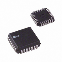
AD698APZ Analog Devices Inc, AD698APZ Datasheet - Page 8

AD698APZ
Manufacturer Part Number
AD698APZ
Description
IC LVDT SIGNAL COND 28-PLCC
Manufacturer
Analog Devices Inc
Type
Signal Conditionerr
Datasheet
1.AD698APZ.pdf
(12 pages)
Specifications of AD698APZ
Input Type
Voltage
Output Type
Voltage
Interface
LVDT
Current - Supply
15mA
Mounting Type
Surface Mount
Package / Case
28-LCC (J-Lead)
Bandwidth
20kHz
Supply Voltage Min
13V
Supply Voltage Max
36V
Digital Ic Case Style
LCC
No. Of Pins
28
Operating Temperature Range
-40°C To +85°C
Msl
MSL 5 - 48 Hours
Supply Voltage Range
13V To 36V
Audio Ic Case Style
PLCC
Base Number
698
Rohs Compliant
Yes
Lead Free Status / RoHS Status
Lead free / RoHS Compliant
Lead Free Status / RoHS Status
Lead free / RoHS Compliant, Lead free / RoHS Compliant
Available stocks
Company
Part Number
Manufacturer
Quantity
Price
Company:
Part Number:
AD698APZ
Manufacturer:
Analog Devices Inc
Quantity:
135
Part Number:
AD698APZ
Manufacturer:
ADI/亚德诺
Quantity:
20 000
AD698
Note that V
value .
Figure 12 shows the desired response.
DESIGN PROCEDURE
SINGLE SUPPLY OPERATION
Figure 13 shows the single supply connection method.
For single supply operation, repeat Steps 1 through 10 of the
design procedure for dual supply operation. R5, R6 and C5 are
additional component values to be determined. V
sured with respect to SIGNAL REFERENCE.
10. Compute a maximum value of R5 and R6 based upon the
V
Figure 12. V
( 0.1 Inch)
Figure 13. Interconnection Diagram for Single Supply
Operation
ps
relationship
+30V
R
6.8µF
S
PHASE LAG
C
A
R
OS
T
C
should
D
B
0.1µF
OUT
C5
R
S
–0.1
(0 V–10 V Full Scale) vs. Displacement
C2
C1
1M
R5 + R6
R1
R6
be chosen so that R3 cannot have negative
R5
V
C
A
PHASE LEAD
OUT
+10
+5
R
C
T
10
11
12
1
2
3
4
5
6
7
8
9
(VOLTS)
B
D
–V
EXC1
EXC2
LEV1
LEV2
FREQ1
FREQ2
BFILT1
BFILT2
–BIN
+BIN
–AIN
R
S
C
S
V
AD698
+0.1d (INCHES)
PS
FEEDBACK
/100 A
OFFSET2
OUT FILT
OFFSET1
+ACOMP
–ACOMP
SIG OUT
SIG REF
PHASE LAG = Arc Tan (Hz RC);
PHASE LEAD = Arc Tan 1/(Hz RC)
WHERE R = R
AFILT2
AFILT1
+AIN
+V
S
19
18
17
16
14
13
24
23
22
20
15
21
R4
R3
S
// (R
R2
C4
C3
OUT
S
A
LAG/LEAD
NETWORK
C
+ R
PHASE
1000pF
REFERENCE
T
is mea-
)
SIGNAL
D
B
V
OUT
R
L
–8–
11. The voltage drop across R5 must be greater than
Therefore
Based upon the constraints of R5 + R6 (Step 10) and R5 (Step
11), select an interim value of R6.
12. Load current through R
13. C5 is a bypass capacitor in the range of 0.1 F to 1 F.
Gain Phase Characteristics
To use an LVDT in a closed-loop mechanical servo application,
it is necessary to know the dynamic characteristics of the trans-
ducer and interface elements. The transducer itself is very quick
to respond once the core is moved. The dynamics arise prima-
rily from the interface electronics. Figures 14, 15 and 16 show
the frequency response of the AD698 LVDT Signal Conditioner.
Note that Figures 15 and 16 are basically the same; the differ-
ence is frequency range covered. Figure 15 shows a wider range
of mechanical input frequencies at the expense of accuracy.
Figure 14. Gain and Phase Characteristics vs. Frequency
(0 kHz–10 kHz)
R6, and flows back to V
tions, make sure the voltage drop across R5 is met as de-
fined in Step 11.
As a final check on the power supply voltages, verify that
the peak values of V
the voltage between +V
R5
2 10 k
–120
–180
–240
–300
–360
–420
–10
–20
–30
–40
–50
–60
–70
–60
10
0
0
2 10 k
0
R2 = 81k
f
2.0µF
R2 = 81k
f
EXC
EXC
= 2.5kHz
= 2.5kHz
R4 2 k
2.0µF
1.2V
R4 2 k
A
1.2V
100
and V
S
L
FREQUENCY – Hz
PS
and –V
100 A
returns to the junction of R5 and
. Under maximum load condi-
0.33µF
B
250 A
are at least 2.5 volts less than
250 A
S
.
1k
0.33µF
4 R2
V
0.1µF
OUT
4 R2
V
OUT
0.1µF
Volts
10k
REV. B
Ohms


