AD693AD Analog Devices Inc, AD693AD Datasheet - Page 10
AD693AD
Manufacturer Part Number
AD693AD
Description
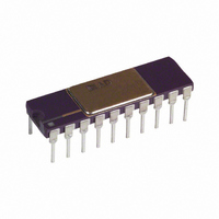
IC SGNL COND 4-20MA TX 20-CDIP
Manufacturer
Analog Devices Inc
Type
Signal Conditionerr
Datasheet
1.AD693AQ.pdf
(12 pages)
Specifications of AD693AD
Rohs Status
RoHS non-compliant
Input Type
Voltage
Output Type
Voltage
Interface
3-Wire
Current - Supply
20mA
Mounting Type
Through Hole
Package / Case
20-CDIP (0.300", 7.62mm)
No. Of Amplifiers
5
Input Offset Voltage
200µV
Cmrr
90dB
Supply Voltage Range
12V To 36V
Supply Current
500µA
Amplifier Case Style
DIP
No. Of Pins
20
Operating Temperature Range
-40°C To +85°C
Rohs Compliant
No
Available stocks
Company
Part Number
Manufacturer
Quantity
Price

Part Number:
AD693AD
Manufacturer:
ADI/亚德诺
Quantity:
20 000


AD693
increasing the application voltages by adding resistance between
Pins 14 and 3 will decrease the temperature span.
An external voltage divider may also be used in conjunction
with the circuit shown to produce any range of temperature
spans as well as providing zero output (4 mA) for a non 0
temperature input. For example, measuring V
voltage 2.385 times the excitation (rather than 2 times) will
result in zero input to the Signal Amplifier when the RTD is at
100 C (or 138.5 ).
As suggested in Table I, the temperature span may also be adjusted
by changing the voltage span of the Signal Amplifier. Changing the
gain from 2 to 4, for example, will halve the temperature span to
about 52 C on the 4-20mA output configuration. (See section
“Adjusting Input Span.”)
The configuration for a three-wire RTD shown in Figure 17 can
accommodate two-wire sensors by simply joining Pins 1 and 5
of the AD693.
INTERFACING LOAD CELLS AND METAL FOIL STRAIN
GAGES
The availability of the on-chip Voltage Reference, Auxiliary
Amplifier and 3 mA of excitation current make it easy to adapt
the AD693 to a variety of load cells and strain gages.
The circuit shown in Figure 18 illustrates a generalized approach in
which the full flexibility of the AD693 is required to interface to a
low resistance bridge. For a high impedance transducer the
bridge can be directly powered from the 6.2 V Reference.
Component values in this example have been selected to match
the popular standard of 2 mV/V sensitivity and 350
resistance. Load cells are generally made for either tension and
compression, or compression only; use of the 12 mA zero tap
allows for operation in the tension and compression mode. An
optional zero adjustment is provided with values selected for
+2% FS adjustment range.
Because of the low resistance of most foil bridges, the excitation
voltage must be low so as not to exceed the available 4 mA zero
current. About 1 V is derived from the 6.2 V Reference and an
Figure 18. Utilizing the Auxiliary Amplifier to Drive a Load Cell, 12 mA
X
with respect to a
bridge
–10–
external voltage divider; the Aux-Amp is then used as a follower
to make a stiff drive for the bridge. Similar applications with
higher resistance sensors can use proportionally higher voltage.
Finally, to accommodate the 2 mV/V sensitivity of the bridge,
the full-scale span of the Signal Amplifier must be reduced.
Using the load cell in both tension and compression with 1 V of
excitation, therefore, dictates that the span be adjusted to 4 mV.
By substituting in the expression, R
the nominal resistance required to achieve this span is found to
be 61.54 . Calculate the minimum resistance required by
subtracting 10% from 61.54
tolerance of the AD693, leaving 55.38
Span.”) The standard value of 54.9
potentiometer for full-scale adjustment.
If a load cell with a precalibrated sensitivity constant is to be
used, the resultant full-scale span applied to the Signal Amplifier is
found by multiplying that sensitivity by the excitation voltage.
(In Figure 18, the excitation voltage is actually (10 k /62.3 k )
(6.2 V) = 0.995 V).
THERMOCOUPLE MEASUREMENTS
The AD693 can be used with several types of thermocouple
inputs to provide a 4-20 mA current loop output corresponding
to a variety of measurement temperature ranges. Cold junction
compensation (CJC) can be implemented using an AD592 or
AD590 and a few external resistors as shown in Figure 19.
From Table II simply choose the type of thermocouple and the
appropriate average reference junction temperature to select
values for R
R
the thermocouple loop voltage. The 50
biased by R
appropriate for the divider and also translates the Kelvin scale of
the AD592 to Celsius. To calibrate the circuit, put the
thermocouple in an ice bath (or use a thermocouple simulator
set to 0) and adjust the potentiometer for a 4 mA loop current.
The span of the circuit in C is determined by matching the
signal amplifier input voltage range to its temperature equivalent
COMP
as a result of the AD592 1 A/K output and is added to
Z
COMP
to provide the correct zero adjustment range
and R
Z
. The CJC voltage is developed across
8 mA Output
to allow for the internal resistor
S1
= 400 /[(30 mV/S) – 1],
is used with a 20
(See “Adjusting Input
potentiometer is
REV. A
Related parts for AD693AD
Image
Part Number
Description
Manufacturer
Datasheet
Request
R

Part Number:
Description:
±1.7g Dual-Axis IMEMS Accelerometer Evaluation Board
Manufacturer:
Analog Devices Inc
Datasheet:

Part Number:
Description:
Inertial Sensor Evaluation System
Manufacturer:
Analog Devices Inc
Datasheet:
Part Number:
Description:
Manufacturer:
Analog Devices Inc
Datasheet:
Part Number:
Description:
Manufacturer:
Analog Devices Inc
Datasheet:
Part Number:
Description:
Manufacturer:
Analog Devices Inc
Datasheet:
Part Number:
Description:
Manufacturer:
Analog Devices Inc
Datasheet:
Part Number:
Description:
Manufacturer:
Analog Devices Inc
Datasheet:
Part Number:
Description:
Manufacturer:
Analog Devices Inc
Datasheet:
Part Number:
Description:
Manufacturer:
Analog Devices Inc
Datasheet:
Part Number:
Description:
Manufacturer:
Analog Devices Inc
Datasheet:
Part Number:
Description:
Manufacturer:
Analog Devices Inc
Datasheet:
Part Number:
Description:
Manufacturer:
Analog Devices Inc
Datasheet:
Part Number:
Description:
Manufacturer:
Analog Devices Inc
Datasheet: