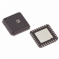
AD9943KCPZ Analog Devices Inc, AD9943KCPZ Datasheet - Page 17

AD9943KCPZ
Manufacturer Part Number
AD9943KCPZ
Description
IC CCD SIGNAL PROCESSOR 32-LFCSP
Manufacturer
Analog Devices Inc
Type
CCD Signal Processor, 10-Bitr
Datasheet
1.AD9943KCPZRL.pdf
(20 pages)
Specifications of AD9943KCPZ
Package / Case
32-LFCSP
Input Type
Logic
Output Type
Logic
Interface
3-Wire Serial
Mounting Type
Surface Mount
Supply Voltage Range
2.7V To 3.6V
Operating Temperature Range
-20°C To +85°C
Digital Ic Case Style
LFCSP
No. Of Pins
32
Svhc
No SVHC (18-Jun-2010)
Supply Voltage
RoHS Compliant
Ic Function
CCD Signal Processor
Rohs Compliant
Yes
Lead Free Status / RoHS Status
Lead free / RoHS Compliant
Current - Supply
-
Lead Free Status / RoHS Status
Lead free / RoHS Compliant
Available stocks
Company
Part Number
Manufacturer
Quantity
Price
Company:
Part Number:
AD9943KCPZ
Manufacturer:
ADI
Quantity:
585
Part Number:
AD9943KCPZ
Manufacturer:
ADI/亚德诺
Quantity:
20 000
Company:
Part Number:
AD9943KCPZRL
Manufacturer:
SANYO
Quantity:
410
Company:
Part Number:
AD9943KCPZRL
Manufacturer:
ADI
Quantity:
15 000
CCD MODE TIMING
OUTPUT
SIGNAL
CLPOB
DATACLK
PBLK
DATA
OUTPUT
CCD
SIGNAL
DATA
CCD
SHD
SHP
NOTES
1. CLPOB WILL OVERWRITE PBLK. PBLK WILL NOT AFFECT CLAMP OPERATION IF OVERLAPPING WITH CLPOB.
2. PBLK SIGNAL IS OPTIONAL.
3. DIGITAL OUTPUT DATA WILL BE ALL ZEROS DURING PBLK. OUTPUT DATA LATENCY IS NINE DATACLK CYCLES.
NOTES
1. RECOMMENDED PLACEMENT FOR DATACLK RISING EDGE IS BETWEEN THE SHD RISING EDGE AND NEXT SHP FALLING EDGE.
2. CCD SIGNAL IS SAMPLED AT SHP AND SHD RISING EDGES.
EFFECTIVE PIXELS
EFFECTIVE PIXEL DATA
t
ID
t
S1
N – 10
t
OD
N
t
ID
N – 9
OPTICAL BLACK PIXELS
t
S2
N + 1
Figure 15. Typical CCD Mode Line Clamp Timing
OB PIXEL DATA
Figure 14. CCD Mode Timing
Rev. B | Page 17 of 20
N – 8
t
CP
N + 2
HORIZONTAL
BLANKING
DUMMY PIXELS
N – 1
DUMMY BLACK
N + 9
AD9943/AD9944
EFFECTIVE PIXELS
EFFECTIVE DATA
N
N + 10


