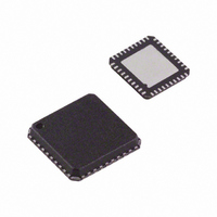
AD9949KCPZ Analog Devices Inc, AD9949KCPZ Datasheet - Page 11

AD9949KCPZ
Manufacturer Part Number
AD9949KCPZ
Description
IC CCD SIGNAL PROCESSOR 40-LFCSP
Manufacturer
Analog Devices Inc
Type
CCD Signal Processor, 12-Bitr
Datasheet
1.AD9949AKCPZ.pdf
(36 pages)
Specifications of AD9949KCPZ
Input Type
Logic
Output Type
Logic
Interface
3-Wire Serial
Mounting Type
Surface Mount
Package / Case
40-LFCSP
Analog Front End Type
CCD
Analog Front End Category
Video
Interface Type
Serial (3-Wire)
Sample Rate
36MSPS
Input Voltage Range
0.5V
Operating Supply Voltage (min)
2.7V
Operating Supply Voltage (typ)
3V
Operating Supply Voltage (max)
3.6V
Resolution
12b
Number Of Adc's
1
Power Supply Type
Analog/Digital
Operating Temp Range
-20C to 85C
Operating Temperature Classification
Commercial
Mounting
Surface Mount
Pin Count
40
Package Type
LFCSP EP
Number Of Channels
1
Lead Free Status / RoHS Status
Lead free / RoHS Compliant
Current - Supply
-
Lead Free Status / RoHS Status
Compliant, Lead free / RoHS Compliant
Available stocks
Company
Part Number
Manufacturer
Quantity
Price
Company:
Part Number:
AD9949KCPZ
Manufacturer:
TI
Quantity:
6 528
Part Number:
AD9949KCPZ
Manufacturer:
ADI/亚德诺
Quantity:
20 000
Company:
Part Number:
AD9949KCPZRL
Manufacturer:
PERICOM
Quantity:
3
SYSTEM OVERVIEW
Figure 11 shows the typical system application diagram for the
AD9949. The CCD output is processed by the AD9949’s AFE
circuitry, which consists of a CDS, a PxGA, a VGA, a black level
clamp, and an ADC. The digitized pixel information is sent to
the digital image processor chip where all postprocessing and
compression occurs. To operate the CCD, CCD timing
parameters are programmed into the AD9949 from the image
processor through the 3-wire serial interface. From the system
master clock, CLI, provided by the image processor, the
AD9949 generates the high speed CCD clocks and all internal
AFE clocks. All AD9949 clocks are synchronized with VD and
HD. The AD9949’s horizontal pulses (CLPOB, PBLK, and
HBLK) are programmed and generated internally.
The H-drivers for H1 to H4 and RG are included in the
AD9949, allowing these clocks to be directly connected to the
CCD. The H-drive voltage of 3 V is supported in the AD9949.
Figure 12 shows the horizontal and vertical counter dimensions
for the AD9949. All internal horizontal clocking is programmed
using these dimensions to specify line and pixel locations.
CCD
CLI
HD
VD
V-DRIVER
H1 TO H4, RG
CCDIN
Figure 11. Typical Application
INTERFACE
SERIAL
INTEGRATED
AD9949
AFE + TD
V1 TO Vx, VSG1 TO VSGx, SUBCK
HD, VD
DOUT
CLI
MAX HD LENGTH IS 4095 PIXELS
DIGITAL IMAGE
PROCESSING
MAX VD LENGTH IS 4095 LINES
Figure 13. Maximum VD/HD Dimensions
ASIC
Rev. B | Page 11 of 36
H-COUNTER BEHAVIOR
When the maximum horizontal count of 4096 pixels is
exceeded, the H-counter in the AD9949 rolls over to zero and
continues counting. It is, therefore, recommended that the
maximum counter value not be exceeded.
However, the newer AD9949A version behaves differently. In
the AD9949A, the internal H-counter holds at its maximum
count of 4095 instead of rolling over. This feature allows the
AD9949A to be used in applications containing a line length
greater than 4096 pixels. Although no programmable values for
the horizontal blanking or clamping are available beyond pixel
4095, the H, RG, and AFE clocking continues to operate,
sampling the remaining pixels on the line.
Figure 12. Vertical and Horizontal Counters
12-BIT VERTICAL = 4096 LINES MAX
12-BIT HORIZONTAL = 4096 PIXELS MAX
MAXIMUM FIELD DIMENSIONS
AD9949


