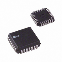
AD698AP Analog Devices Inc, AD698AP Datasheet - Page 10

AD698AP
Manufacturer Part Number
AD698AP
Description
IC LVDT SIGNAL COND 28-PLCC
Manufacturer
Analog Devices Inc
Type
Signal Conditionerr
Datasheet
1.AD698APZ.pdf
(12 pages)
Specifications of AD698AP
Rohs Status
RoHS non-compliant
Input Type
Voltage
Output Type
Voltage
Interface
LVDT
Current - Supply
15mA
Mounting Type
Surface Mount
Package / Case
28-LCC (J-Lead)
Bandwidth
20kHz
Supply Voltage Min
13V
Supply Voltage Max
36V
Digital Ic Case Style
LCC
No. Of Pins
28
Operating Temperature Range
-40°C To +85°C
Msl
MSL 5 - 48 Hours
Lead Free Status / RoHS Status
Contains lead / RoHS non-compliant
Available stocks
Company
Part Number
Manufacturer
Quantity
Price
Company:
Part Number:
AD698APZ
Manufacturer:
Analog Devices Inc
Quantity:
135
Part Number:
AD698APZ
Manufacturer:
ADI/亚德诺
Quantity:
20 000
AD698
Determining LVDT Sensitivity
LVDT sensitivity can be determined by measuring the LVDT
secondary voltages as a function of primary drive and core posi-
tion, and performing a simple computation.
Energize the LVDT at its recommended primary drive level,
V
mechanical full-scale position and measure secondary voltages
V
From Figure 19,
Thermal Shutdown and Loading Considerations
The AD698 is protected by a thermal overload circuit. If the die
temperature reaches 165 C, the sine wave excitation amplitude
gradually reduces, thereby lowering the internal power dissipa-
tion and temperature.
Due to the ratiometric operation of the decoder circuit, only
small errors result from the reduction of the excitation ampli-
tude. Under these conditions the signal-processing section of
the AD698 continues to meet its output specifications.
The thermal load depends upon the voltage and current deliv-
ered to the load as well as the power supply potentials. An
LVDT Primary will present an inductive load to the sine wave
excitation. The phase angle between the excitation voltage and
current must also be considered, further complicating thermal
calculations.
APPLICATIONS
Most of the applications for the AD598 can also be imple-
mented with the AD698. Please refer to the applications written
for the AD598 for a detailed explanation.
See AD598 data sheet for:
– Proving Ring-Weigh Scale
– Synchronous Operation of Multiple LVDTs
– High Resolution Position-to-Frequency Circuit
PRI
A
and V
Figure 19. LVDT Secondary Voltage vs. Core
Displacement
(3 V rms for the E100). Set the core displacement to its
B
Sensitivity
.
d = –100 mils
Sensitivity
V
SEC
3 V
WHEN V
0.72
d = 0
100 mils
PRI
V
SECONDARY
3V rms
V
d = +100 mils
PRI
2.4 mV /V mil
1.71V rms
V
0.99V rms
V
d
A
B
–10–
– Low Cost Setpoint Controller
– Mechanical Follower Servo Loop
– Differential Gaging and Precision Differential Gaging
AC BRIDGE SIGNAL CONDITIONER
Bridge circuits which use dc excitation are often plagued by er-
rors caused by thermocouple effects, 1/f noise, dc drifts in the
electronics, and line noise pickup. One way to get around these
problems is to excite the bridge with an ac waveform, amplify
the bridge output with an ac amplifier, and synchronously de-
modulate the resulting signal. The ac phase and amplitude in-
formation from the bridge is recovered as a dc signal at the
output of the synchronous demodulator. The low frequency
system noise, dc drifts, and demodulator noise all get mixed to
the carrier frequency and can be removed by means of a low-
pass filter.
The AD698 with the addition of a simple ac gain stage can be
used to implement an ac bridge. Figure 20 shows the connec-
tions for such a system. The AD698 oscillator provides ac
excitation for the bridge. The low level bridge signal is amplified
by the gain stage created by A1, A2 to provide a differential in-
put to the A Channel of the AD698. The signal is then synchro-
nously detected by A Channel. The B Channel is used to detect
the level of the bridge excitation. The ratio of A/B is then calcu-
lated and converted to an output voltage by R2. An optional
phase lag/lead network can be added in front of the A compara-
tor to adjust for phase delays through the bridge and the ampli-
fier, or if the phase delay is small, it can be ignored or compensated
for by a gain adjustment.
This circuit can be used for resistive bridges such as strain
gages, or for inductive or capacitive bridges that are commonly
used for pressure or flow sensors. The low level signal outputs of
these sensors are susceptible to noise and interference and are
good candidates for ac signal processing techniques.
Component Selection
Amplifiers A1, A2 will be chosen depending on the type of
bridge that is conditioned. Capacitive bridges should use an
amplifier with low bias current; a large bleeder resistor will be
required from the amplifier inputs to ground to provide a path
for the dc bias current. Resistive and inductive bridges can use a
more general purpose amplifier. The dc performance of A1, A2
are not as important as their ac performance. DC errors such as
voltage offset will be chopped out by the AD698 since they are
not synchronous to the carrier frequency.
The oscillator amplitude and span resistor for the AD698 may
be chosen by first computing the transfer function or sensitivity
of the bridge and the ac amplifier. This ratio will correspond to
the A/B term in the AD698 transfer function. For example, sup-
pose that a resistive strain gage with a sensitivity, S, of 2 mV/V
at full scale is used. Select an arbitrary target value for A/B that
is close to its maximum value such as A/B = 0.8. Then choose a
gain for the ac amplifier so that the strain gage transfer function
from excitation to output also equals 0.8. Thus the required am-
plifier gain will be [A/B]/ S; or 0.8/ 0.002 V/V = 400. Then
select values for R
S
and R
G
. For the gain stage:
REV. B


