AD698AP Analog Devices Inc, AD698AP Datasheet - Page 3
AD698AP
Manufacturer Part Number
AD698AP
Description
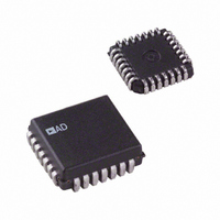
IC LVDT SIGNAL COND 28-PLCC
Manufacturer
Analog Devices Inc
Type
Signal Conditionerr
Datasheet
1.AD698APZ.pdf
(12 pages)
Specifications of AD698AP
Rohs Status
RoHS non-compliant
Input Type
Voltage
Output Type
Voltage
Interface
LVDT
Current - Supply
15mA
Mounting Type
Surface Mount
Package / Case
28-LCC (J-Lead)
Bandwidth
20kHz
Supply Voltage Min
13V
Supply Voltage Max
36V
Digital Ic Case Style
LCC
No. Of Pins
28
Operating Temperature Range
-40°C To +85°C
Msl
MSL 5 - 48 Hours
Lead Free Status / RoHS Status
Contains lead / RoHS non-compliant
Available stocks
Company
Part Number
Manufacturer
Quantity
Price

Company:
Part Number:
AD698APZ
Manufacturer:
Analog Devices Inc
Quantity:
135
Part Number:
AD698APZ
Manufacturer:
ADI/亚德诺
Quantity:
20 000


NOTES
1
2
3
4
5
6
7
8
Specifications subject to change without notice.
Specifications shown in boldface are tested on all production units at final electrical test. Results from those tested are used to calculate outgoing quality levels.
All min and max specifications are guaranteed, although only those shown in boldface are tested on all production units.
CAUTION
ESD (electrostatic discharge) sensitive device. Electrostatic charges as high as 4000 V readily
accumulate on the human body and test equipment and can discharge without detection.
Although the AD698 features proprietary ESD protection circuitry, permanent damage may
occur on devices subjected to high energy electrostatic discharges. Therefore, proper ESD
precautions are recommended to avoid performance degradation or loss of functionality.
REV. B
Model
AD698AP
AD698SQ
ABSOLUTE MAXIMUM RATINGS
Total Supply Voltage (+V
Storage Temperature Range
Operating Temperature Range
Lead Temperature Range (Soldering 60 sec) . . . . . . . . +300 C
Power Dissipation Derates above +65 C
THERMAL CHARACTERISTICS
P Package 30 C/W
Q Package 26 C/W
A and B represent the Mean Average Deviation (MAD) of the detected sine waves V
Nonlinearity of the AD698 only in units of ppm of full scale. Nonlinearity is defined as the maximum measured deviation of the AD698 output voltage from a
See Transfer Function.
For example, if the excitation to the primary changes by 1 dB, the gain of the system will change by typically 100 ppm.
Output ripple is a function of the AD698 bandwidth determined by C1 and C2. A 1000 pF capacitor should be connected in parallel with R2 to reduce the output
R1 is shown in Figures 7, 8 and 13.
Excitation voltage drift is not an important specification because of the ratiometric operation of the AD698.
From T
multiply V
straight line. The straight line is determined by connecting the maximum produced full-scale negative voltage with the maximum produced full-scale positive voltage.
ripple. See Figures 7, 8 and 13.
error for the AD698AP from T
(20 ppm/ C
P Package . . . . . . . . . . . . . . . . . . . . . . . . . –65 C to +150 C
Q Package . . . . . . . . . . . . . . . . . . . . . . . . –65 C to +150 C
AD698SQ . . . . . . . . . . . . . . . . . . . . . . . . –55 C to +125 C
AD698AP . . . . . . . . . . . . . . . . . . . . . . . . . –40 C to +85 C
P Package . . . . . . . . . . . . . . . . . . . . . . . . . . . . . . . 12 mW/ C
Q Package . . . . . . . . . . . . . . . . . . . . . . . . . . . . . . 12 mW/ C
MIN
OUT
to T
65 C) + Offset Drift from –40 C to +25 C (5 ppm/ C
MAX
JC
+1 for A
Package Description
28-Pin PLCC
24-Pin Double Cerdip
the overall error due to the AD698 alone is determined by combining gain error, gain drift and offset drift. For example, the typical overall
COMP+
ORDERING GUIDE
60 C/W
62 C/W
MIN
JA
S
> A
to –V
to T
COMP–
MAX
S
, and V
) . . . . . . . . . . . . . . . . . 36 V
is calculated as follows: Overall Error = Gain Error at +25 C ( 0.2% Full Scale) + Gain Drift from –40 C to +25 C
OUT
–1 for A
Package Option
P-28A
Q-24A
COMP–
> A
65 C) = 0.36% of full scale. Note that 1000 ppm of full scale equals 0.1% of full scale.
COMP+
.
–3–
A
and V
B
. The polarity of V
BFILT1
BFILT2
FREQ1
FREQ2
NC = NO CONNECT
LEV1
LEV2
NC
10
11
5
6
7
8
9
CONNECTION DIAGRAMS
FREQ1
FREQ2
BFILT1
BFILT2
EXC1
EXC2
LEV1
LEV2
OUT
–BIN
+BIN
–AIN
12 13 14 15 16 17 18
–V
4
S
is affected by the sign of the A comparator, i.e.,
3
10
11
12
24-Pin Cerdip
1
2
3
4
5
6
7
8
9
28-Pin PLCC
(Not to Scale)
(Not to Scale)
TOP VIEW
2
TOP VIEW
AD698
AD698
1
28 27 26
WARNING!
16
24
23
22
21
20
19
18
17
15
14
13
+V
OFFSET1
OFFSET2
SIG REF
SIG OUT
FEEDBACK
OUT FILT
AFILT1
AFILT2
–ACOMP
+ACOMP
+AIN
S
25
24
23
22
20
19
21
ESD SENSITIVE DEVICE
NC
SIG REF
SIG OUT
FEEDBACK
OUT FILT
AFILT1
AFILT2
AD698
Related parts for AD698AP
Image
Part Number
Description
Manufacturer
Datasheet
Request
R

Part Number:
Description:
±1.7g Dual-Axis IMEMS Accelerometer Evaluation Board
Manufacturer:
Analog Devices Inc
Datasheet:

Part Number:
Description:
Inertial Sensor Evaluation System
Manufacturer:
Analog Devices Inc
Datasheet:
Part Number:
Description:
Manufacturer:
Analog Devices Inc
Datasheet:
Part Number:
Description:
Manufacturer:
Analog Devices Inc
Datasheet:
Part Number:
Description:
Manufacturer:
Analog Devices Inc
Datasheet:
Part Number:
Description:
Manufacturer:
Analog Devices Inc
Datasheet:
Part Number:
Description:
Manufacturer:
Analog Devices Inc
Datasheet:
Part Number:
Description:
Manufacturer:
Analog Devices Inc
Datasheet:
Part Number:
Description:
Manufacturer:
Analog Devices Inc
Datasheet:
Part Number:
Description:
Manufacturer:
Analog Devices Inc
Datasheet:
Part Number:
Description:
Manufacturer:
Analog Devices Inc
Datasheet:
Part Number:
Description:
Manufacturer:
Analog Devices Inc
Datasheet:
Part Number:
Description:
Manufacturer:
Analog Devices Inc
Datasheet: